Light-emitting device having a patterned substrate

a light-emitting diode and substrate technology, applied in the direction of semiconductor devices, basic electric elements, electrical appliances, etc., can solve the problems of limiting the application of sapphire in high-power (i.e., high brightness) light-emitting diodes, poor heat dissipation properties of light-emitting diodes made of gallium nitride-based materials, etc., to achieve improved light extraction efficiency, high light reflectivity, and improved luminous efficiency of light-eras

Active Publication Date: 2015-10-27
WUXI CHINA RESOURCES HUAJING MICROELECTRONICS
View PDF14 Cites 20 Cited by
  • Summary
  • Abstract
  • Description
  • Claims
  • Application Information

AI Technical Summary

Benefits of technology

[0055]The Light-Emitting Diode device and the manufacturing method thereof disclosed by the present disclosure have the following advantages: (1) the use of the mirror-treated P-type electrode with high light reflectivity as the reflective layer improves the luminous efficiency of the Light-Emitting Diode device; (2) since the N-type electrode has the grid shape and the P-type electrode is within each grid unit of the grid-shaped N-type electrode, a wiring electrode of a big area can be omitted, thereby improving the light extraction efficiency; (3) since the bonding pad is located on the patterned substrate rather than on the LED chip, the wiring for the bonding pad is easier than the conventional wiring on the chip; (4) since the P-type electrode with a big area and high light reflectivity is used, an additional extension layer (e.g., an ITO layer, a ZnO layer, etc.) can be eliminated, thereby optimizing the manufacturing process; and (5) a distributed structure of the P-type electrode and the N-type electrode is advantageous for the extension of the current in the P-type gallium nitride, thereby improving an external quantum efficiency and increasing the light efficiency.

Problems solved by technology

However, there exist the following problems in the technical solutions of the prior art.
Due to the poor thermal conductivity and electrical conductivity of the sapphire, the Light-Emitting Diode device made of the gallium nitride-based material has a poor heat dissipation property, a short lifespan and a complicated manufacturing process, thus limiting the application of the sapphire in high power (i.e., high brightness) Light-Emitting Diodes.
Furthermore, for a gallium nitride-based Light-Emitting Diode (GaN-based LED) device having a structure with a horizontal formal electrode, a P-type electrode will block light, thus the P-type electrode is required to have a good ITO extension layer, resulting in a low light efficiency and a complicated manufacturing process of the GaN-based LED device.
However, although the improved solution effectively solves the above problems of heat dissipation and light blocking, silicon carbide is difficult to process and is even more costly than the sapphire, thereby restricting the application and promotion of the improved solution.
However, due to the use of the reflective metallic layer and the bonding technology, the another one of the existing improved solutions is defective in that: process difficulty and costs are increased, a chip of a structure with formal electrodes cannot be used for manufacturing the Light-Emitting Diode device, an electrode in the light emitting surface blocks light to be emitted so that the light extraction efficiency is reduced, and the wiring for the LED chip is difficult.

Method used


Image

  • Light-emitting device having a patterned substrate
  • Light-emitting device having a patterned substrate
  • Light-emitting device having a patterned substrate

Examples


Embodiment Construction

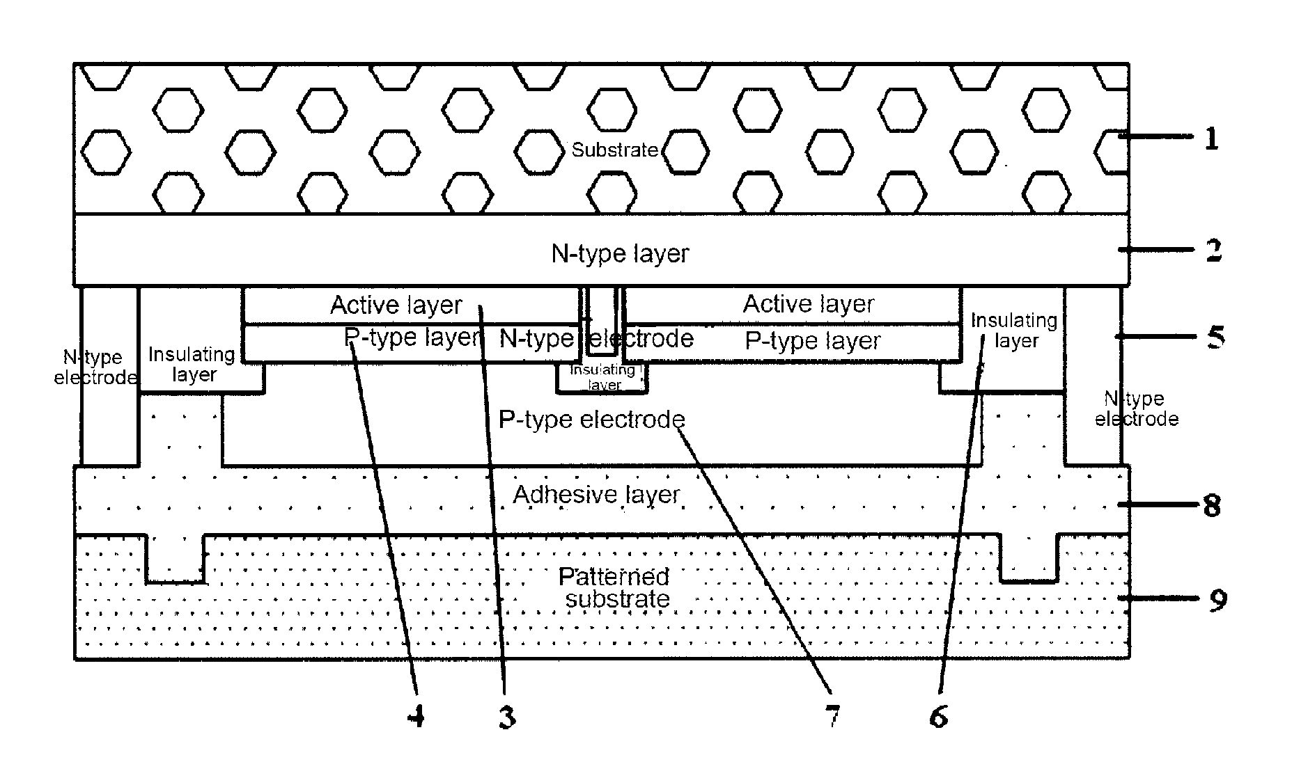
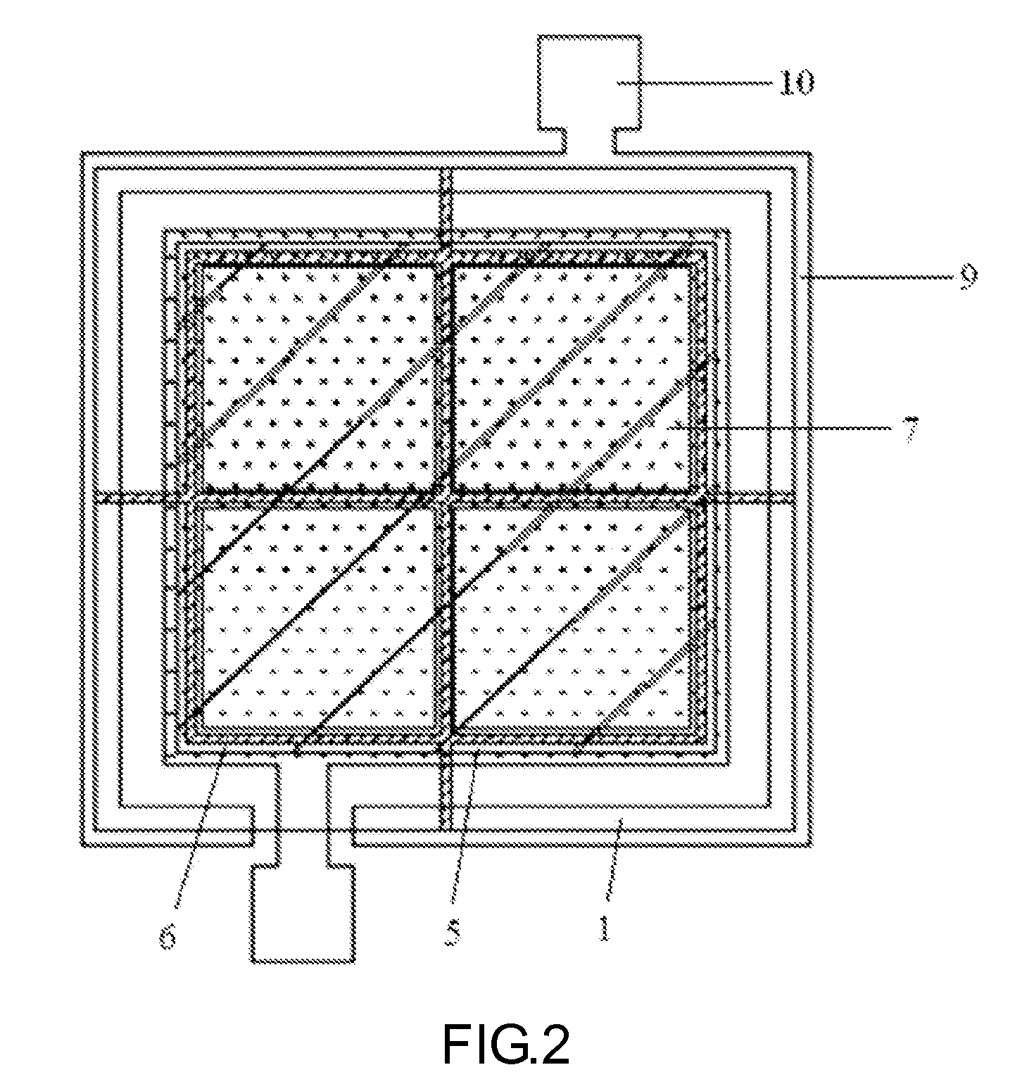
[0060]FIG. 1 is a schematic cross-sectional view of a Light-Emitting Diode device according to an embodiment of the present invention. As shown in FIG. 1, the Light-Emitting Diode device disclosed by the present disclosure includes: a substrate 1; an epitaxial layer located on one side of the substrate 1, where the epitaxial layer includes an N-type layer 2, a P-type layer 4, and an active layer 3 between the N-type layer and the P-type layer; an N-type electrode 5, which is in ohmic contact with one side of the N-type layer that is away from the substrate; a P-type electrode 7, which is in ohmic contact with one side of the P-type layer that is away from the substrate; an adhesive layer 8, one side of which is electrically adhered to both one side of the N-type electrode 5 that is away from the N-type layer 2 and one side of the P-type electrode 7 that is away from the P-type layer 4; and a patterned substrate 9 electrically adhered to the other side of the adhesive layer 8. The Li...


PUM


Abstract

A light-emitting diode device and a manufacturing method thereof. The light-emitting diode device includes: a substrate (1); an epitaxial layer at one side of the substrate (1) and including an N-type layer (2), a P-type layer (4), and an active layer (3) between the N-type layer (2) and the P-type layer (4); an N-type electrode (5); a P-type electrode (7); an adhesive layer (8); and a patterned substrate (9). The light-emitting diode device further includes an insulating layer (6) between the N-type electrode (5) and the P-type electrode (7), the insulating layer (6) electrically insulating the N-type electrode (5) and the P-type electrode (7). In the light-emitting diode device and the manufacturing method thereof, light-emitting efficiency and luminous efficiency of the light-emitting diode device can be improved, wiring is easier as compared with conventional chips, and the manufacturing process can be optimized.

Description

[0001]This application claims priority to a Chinese patent application No. 201210127827.X filed on Apr. 27, 2012 and titled “Light-Emitting Diode Device And Manufacturing Method Thereof”, which is incorporated herein by reference in its entirety.FIELD OF THE INVENTION[0002]The present disclosure relates to a Light-Emitting Diode (LED) device and a manufacturing method thereof, and in particularly to a high power Light-Emitting Diode device with an improved light efficiency and a manufacturing method thereof.BACKGROUND OF THE INVENTION[0003]A Light-Emitting Diode device is a well-known solid state lighting element, which emits light once if a voltage is applied thereto. The Light-Emitting Diode device generally includes a diode region (which is usually called as an epitaxial layer) which includes an N-type layer, a P-type layer and a P-N junction, where an anode contact is in ohmic contact with the P-type layer and a cathode contact is in ohmic contact with the N-type layer. Typicall...

Claims


Application Information

Patent Timeline
Patent Type & Authority Patents(United States)
IPC IPC(8): H01L33/38H01L33/08
CPCH01L33/38H01L33/08H01L33/385H01L33/0075H01L33/22H01L33/62H01L2933/0016H01L2933/0066
Inventor WANG, LEILI, GUOQIYU, ZHIYANPU, RONGSHENG
Owner WUXI CHINA RESOURCES HUAJING MICROELECTRONICS
Why Eureka
Try Eureka