Group 13 element nitride layer, free-standing substrate, functional element, and method of producing group 13 element nitride layer
- Summary
- Abstract
- Description
- Claims
- Application Information
AI Technical Summary
Benefits of technology
Problems solved by technology
Method used
Image
Examples
##ventive example 1
Inventive Example 1
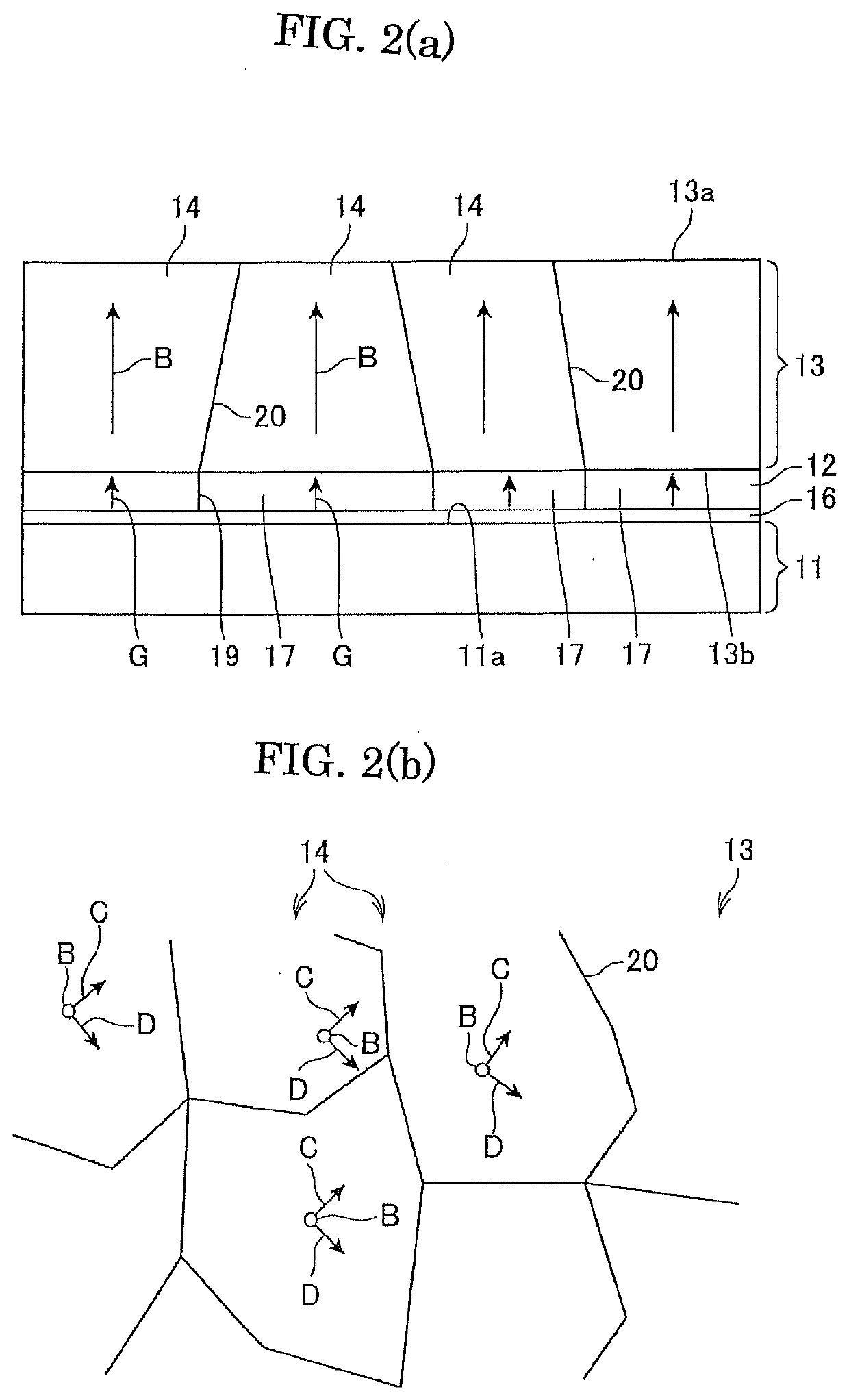
[0099]It was grown the crystal layer of the group 13 nitride of the inventive example, according to the method described referring to FIG. 2.
(Growth of Alumina Layer and Seed Crystal Film)
[0100]Specifically, it was formed an alumina layer 16 having a thickness of 1500 angstrom by sputtering on a C-plane monocrystalline sapphire substrate 11. Specifically, the film-formation was performed by RF magnetron sputtering method at an RF power of 500 W and at a pressure of 1 Pa, by using alumina (purity of 99 percent or higher) as a target and by flowing argon as a process gas (flow rate of 20 sccm), while the C-plane monocrystalline sapphire substrate 11 was heated at 500° C.
[0101]It was then formed the seed crystal layer 12 on the alumina layer 16 by applying MOCVD method. Specifically, a low-temperature GaN layer was formed at 530° C. in 40 nm, followed by depositing a GaN layer at 1050° C. in a thickness of 3 μm to obtain a seed crystal substrate.
[0102](Film Formation...
##ventive example 2
Inventive Example 2
[0152]It was produced the free-standing substrate of gallium nitride crystal layer, according to the same procedure as that of the inventive example 1. However, the full width at half maximum of the (1000) plane reflection of the X-ray rocking curve on the upper surface of the free-standing substrate according to the inventive example 2 was proved to be 11100 arcsec (seconds).
[0153]Meanwhile, the full width at half maximum could be adjusted by changing the thickness of the alumina layer by the sputtering as shown below.
Inventive example 1: 1500 angstrom
Inventive example 2: 1000 angstrom
Inventive example 3: 500 angstrom
Inventive example 4: 150 angstrom
[0154]Dark spots on the uppermost surface of the thus obtained free-standing substrate was counted by cathode luminescence, according to the same procedure as that of the inventive example 1. As a result, the dislocation was not counted and pits were not observed, in the visual field (80×105 μm) to be measured.
[0155]1...
##ventive example 3
Inventive Example 3
[0157]It was produced the free-standing substrate of gallium nitride crystal layer, according to the same procedure as that of the inventive example 1. However, the full width at half maximum of the (1000) plane reflection of the X-ray rocking curve on the upper surface of the free-standing substrate according to the inventive example 3 was proved to be 7500 arcsec (seconds).
[0158]Dark spots on the uppermost surface of the thus obtained free-standing substrate was counted by cathode luminescence, according to the same procedure as that of the inventive example 1. As a result, the dislocation was not counted and pits were not observed, in the visual field (80×105 μm) to be measured.
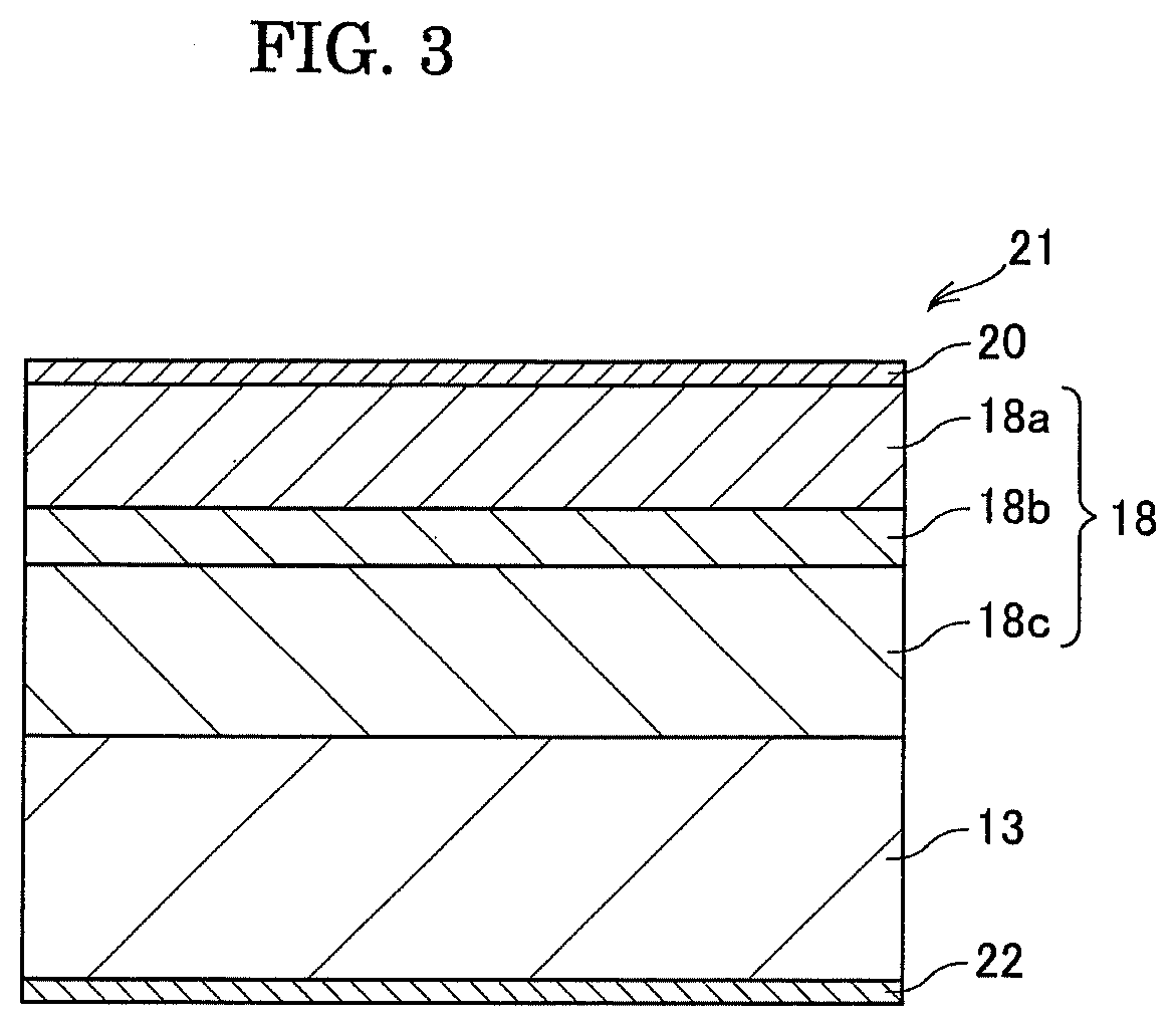
[0159]Further, the light-emitting device was produced on the upper surface of the free-standing substrate.
[0160]100 counts of samples arbitrarily selected from the produced devices were then subjected to I-V measurement by flowing current between the cathode and anode electrodes, and rec...
PUM
| Property | Measurement | Unit |
|---|---|---|
| Time | aaaaa | aaaaa |
| Time | aaaaa | aaaaa |
| Angle | aaaaa | aaaaa |
Abstract
Description
Claims
Application Information


