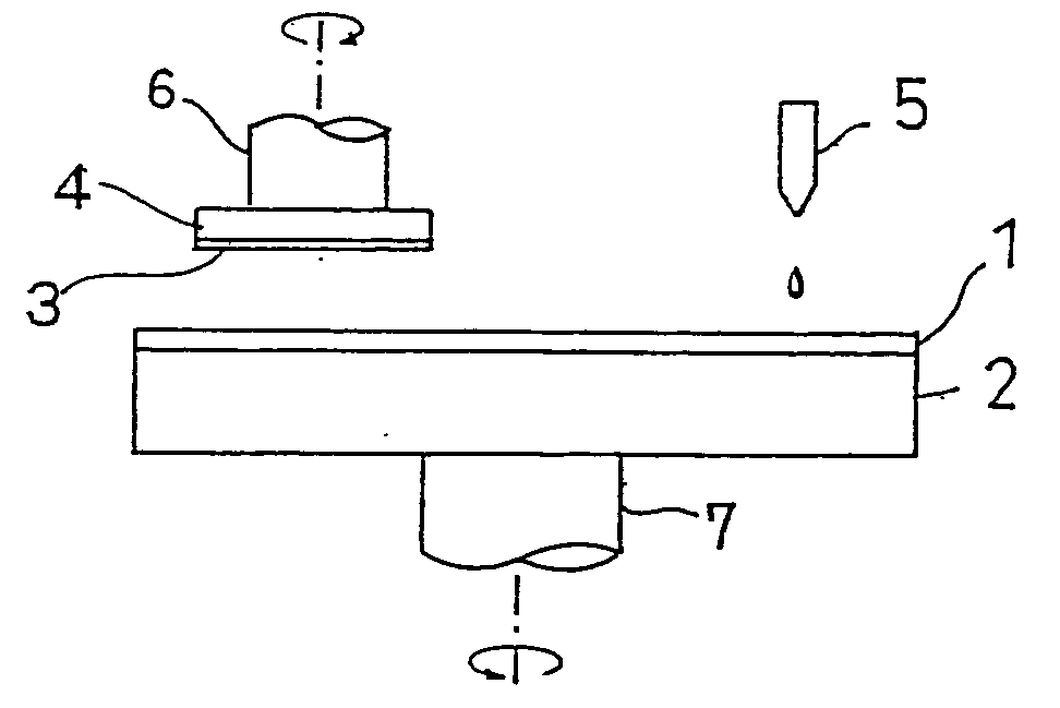
However, the polishing pads described above suffer from the following problems: (a) For the uniformity of whole surface, the elastic
polyurethane layer in the polishing pad described in U.S. Pat. No. 3,504,457 plays a role in making loading applied to a wafer uniform, and soft synthetic leather is used in the outermost polishing layer, and therefore there is no problem such as scratches, but there is the problem of poor planarizing characteristics in minute regions.
Further, the polishing layer has a rigid foamed
polyurethane layer and is thus superior to the synthetic leather in planarizing characteristics, but does not reach levels required in recent years for improving planarizing characteristics in minute regions and for polishing metal films.
The planarizing characteristics can be improved by further increasing the
hardness of the rigid urethane layer, but in this case, scratches occur frequently, thus making this prior art pad unpractical.
(d) The basic idea in the polishing pad described in JP-A 10-156724 is the same as in the art described in JP-A 6-77185, and the range of the
elastic modulus of each layer is limited to achieve a more efficient range, but in this art, there is no description of any substantial realizing means, thus making production of the polishing pad difficult.
However, the step for dividing the layer costs much, thus failing to provide an inexpensive polishing pad.
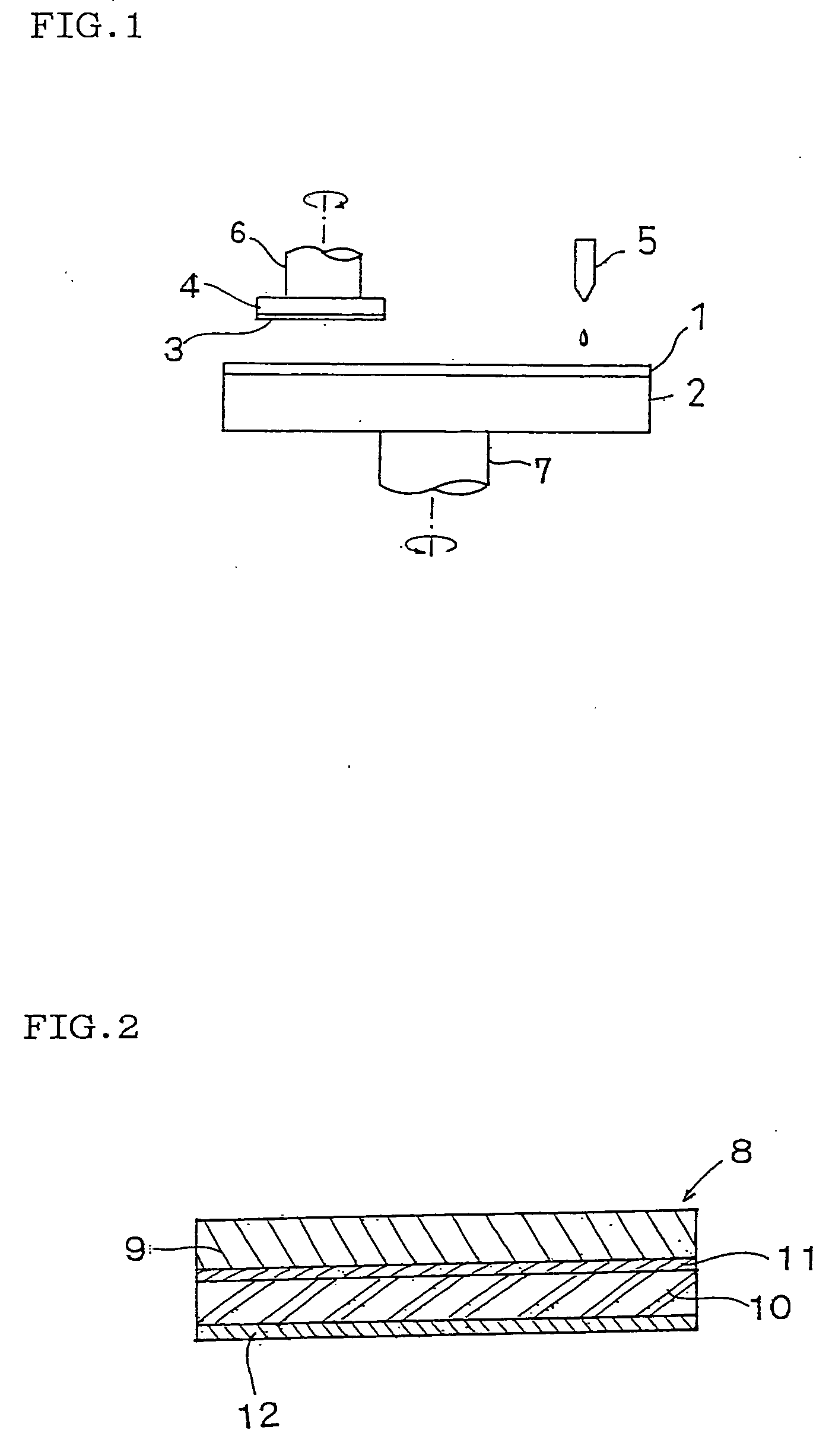
In the case of the polishing pads described in these prior art literatures, the polishing pads are generally stuck via an
adhesive such as a double-coated tape on a polishing
machine used, but their adhesiveness in this case is scarcely examined up to now.
In the case of the polishing pad used generally and widely at present, the removal of the polishing pad from a polishing
machine after use requires very large force, and the exchange of the polishing pad with a new one requires severe hard work.
When the polishing pad is poor in dimensional stability, a change in dimension of the polishing pad occurs due to frictional heat generated in a polishing process, which can cause deterioration in planarizing characteristics.
Conventionally, a polishing pad is often rendered highly elastic for the purpose of improving the planarity of a material to be polished, and there is no sufficient discussion on the dimensional stability of the polishing pad.
However, when the conventional
polyurethane foam sheet is used as a polishing pad or a polishing layer of a polishing pad, the polishing efficiency is improved by increasing the polishing rate, but after polishing, resistance upon removal of a wafer from the polishing pad is increased to generate dechucking error to cause problems of wafer breakage and reduction of operational efficiency.
However, when the polishing rate of the polishing pad during use is changed, it is necessary to regulate the polishing conditions, resulting in low polishing efficiency.
However, when fine particles or hollow fine particles of water-soluble resin, or
polystyrene foamed beads, are dispersed in resin in the known polishing pads described above, uneven dispersion of the particles occur readily due to e.g. a difference in density from the polyurethane as matrix resin.
On the other hand, when a polishing pad consisting of foamed polyurethane obtained by reacting and curing an
isocyanate group-containing compound with an active
hydrogen group-containing compound is used, sufficient polishing performance may not be obtained even if the same components are used, and thus there is demand for improvement.
This increase in temperature changes the
hardness (modulus of elasticity) of the polishing pad, thus exerting adverse influence on planarizing
processing requiring a high degree of surface planarity.
However, it cannot be said that the planarity of this polishing pad comprising high-pressure-gas-containing hollow fine spheres dispersed therein is sufficiently satisfactory.
However, when such a hard pad is used, there occurs a problem of scratches on the polished surface of a workpiece, as described in the above literature (ibid.).
Further, the polishing pad in a non-foam
system cannot sufficiently maintain
slurry abrasive grains on the surface of the pad at the time of polishing, and is thus not preferable from the viewpoint of polishing rate.
However, the characteristics of this polishing pad depend greatly on the water-soluble material, and scratches caused by the
thermoplastic polymer as a major component of the polishing pad cannot be solved.
When the polishing pad is poor in
wetting properties with polishing
slurry, the polishing
slurry cannot sufficiently spread on the polishing pad, and in an extreme case, the polishing pad repels the polishing slurry to reduce the polishing rate significantly thus necessitating a long time for polishing.
Even if the polishing slurry spreads on the polishing pad, the amount of the adhering polishing slurry is uneven, thus failing to uniformly polish an object of polishing.
Further, dry regions may occur on the polishing pad, and when a small amount of polishing slurry adheres to such regions, the solution only is removed by
evaporation etc., resulting in aggregation of
abrasive grains on the regions, which can cause scratches as defects on the surface of a
semiconductor wafer.
On the other hand, when the polishing pad is too excellent in
wetting properties with polishing slurry, the solution in the polishing slurry is absorbed into the surface of the polishing pad, resulting in swelling of the polishing pad to deteriorate the stability of polishing rate.
For the purpose of improving the planarity of an object of polishing, the polishing pad is often rendered highly elastic, and there was no sufficient discussion on the
wetting properties of the polishing pad.
Accordingly, chemicals for
hydrophilization treatment are necessary in producing the polishing pad, and the step of
hydrophilization treatment is also necessary, thus hardly coping with demand for reduction in costs.
However, the polyurethane foamed sheet is excellent in topical planarizing performance, but is poor in
cushioning properties due to a low
compressibility of about 0.5 to 1.0%, thus hardly giving uniform pressure on the whole surface of a wafer.
As a result, the
hardness,
compressibility etc. of the
cushion layer are changed, the characteristics of the whole polishing pad are changed, and polishing characteristics such as uniformity and polishing rate are changed with time to cause a problem of a reduction in wafer yield.
In the technique described in Japanese Patent No. 2842865, however, the polishing layer should be in a such special shape as to cover a side of a
cushion layer, and the backside of the polishing layer should form a concave so as to embed and laminate the
cushion layer therein, thus significantly reducing the productivity of the polishing pad.
In the technique disclosed in Japanese Patent No. 3152188, a waterproof material layer is arranged between polishing
layers, and when the polishing surface approaches the waterproof material layer as the polishing layer is abraded during polishing, the difference in rigidity between the polishing layer and waterproof material layer comes to be significant, to exert adverse influence on the polishing characteristics.

