Manufacturing method of a silicon carbide semiconductor device

a manufacturing method and silicon carbide technology, applied in semiconductor devices, semiconductor/solid-state device details, electrical apparatus, etc., can solve the problems of etching failure, device prone to dielectric breakdown, and actual manufacturing processes for implementing or implementing products of sic power devices still have many and various problems to be solved, so as to increase the breakdown voltage and smooth curved etched surfaces

Inactive Publication Date: 2011-12-06
FUJI ELECTRIC CO LTD
View PDF10 Cites 222 Cited by
  • Summary
  • Abstract
  • Description
  • Claims
  • Application Information

AI Technical Summary

Benefits of technology

[0010]The present invention has been made in view of the above problems, and an object of the invention is therefore to provide a manufacturing method of a silicon carbide semiconductor device including a dry etching method which is necessary in manufacturing a high-breakdown-voltage device and which can increase the breakdown voltage by suppressing generation of micro-masks and thereby produce smoothly curved etched surfaces in forming a mesa groove which is as deep as 10 μm or more and reaches a SiC substrate past a drift layer.
[0011]In the invention, an Al film and a Ni film are laid on an SiC substrate in this order and wet-etched, whereby a two-layer etching mask is formed in which a Ni film portion overhangs an Al film portion. When a mesa groove is formed by dry etching using this etching mask, the rate of incidence of ions of an etching gas on the groove side walls and their vicinities is lowered by virtue of the Ni film portion which overhangs the Al film portion. This reduces the degree of a phenomenon that deep sub-trenches tend to be formed locally in the groove side walls and in their vicinities, and thereby provides an advantage that the breakdown voltage is increased.
[0017]As such the invention can provide a manufacturing method of a silicon carbide semiconductor device including a dry etching method which is necessary in manufacturing a high-breakdown-voltage device and which can increase the breakdown voltage by suppressing generation of micro-masks and thereby producing smoothly curved etched surfaces in forming a mesa groove which is as deep as 10 μm or more and reaches a SiC substrate past a drift layer.

Problems solved by technology

As a result, it is expected that power devices having an SiC substrate can satisfy both high breakdown voltage and low on-resistance, which is difficult for Si devices because of a tradeoff relationship between these two parameters.
However, actual manufacturing processes for putting into practice or implementing as products SiC power devices still have many and various problems to be solved.
One specific problem resides in a process of forming, for example, a trench for a trench gate or a mesa groove having a junction end portion surface which surrounds a device active portion by dry etching in manufacturing a device using a SiC substrate.
That is, in dry etching a SiC substrate, if kinds of gases used for the etching and various etching conditions (ICP (induction-coupled plasma) power, bias power, gas pressure, and gas flow rates) are not controlled properly, an etching failure occurs because an etching mask material is stuck to an etching subject material (formation of micro-masks) during dry etching of mesa grooves or micro-trenches are formed (i.e., small grooves are formed by excessive etching at bottom corners of recesses formed by the etching).
If such acute-angled portions are formed in the surfaces of a mesa groove, an electric field is concentrated which makes any resulting device prone to dielectric breakdown.
That is, the breakdown voltage of the device cannot be increased.
However, this two-stage etching method has problems because the process is complex and there still remains some doubt about its reproducibility.

Method used


Image

  • Manufacturing method of a silicon carbide semiconductor device
  • Manufacturing method of a silicon carbide semiconductor device
  • Manufacturing method of a silicon carbide semiconductor device

Examples


Embodiment Construction

[0024]A manufacturing method of a silicon carbide semiconductor device according to an embodiment of the invention will be hereinafter described in detail with reference to the drawings. Various changes and modifications to the following embodiment are possible without departing from the spirit and scope of the invention.

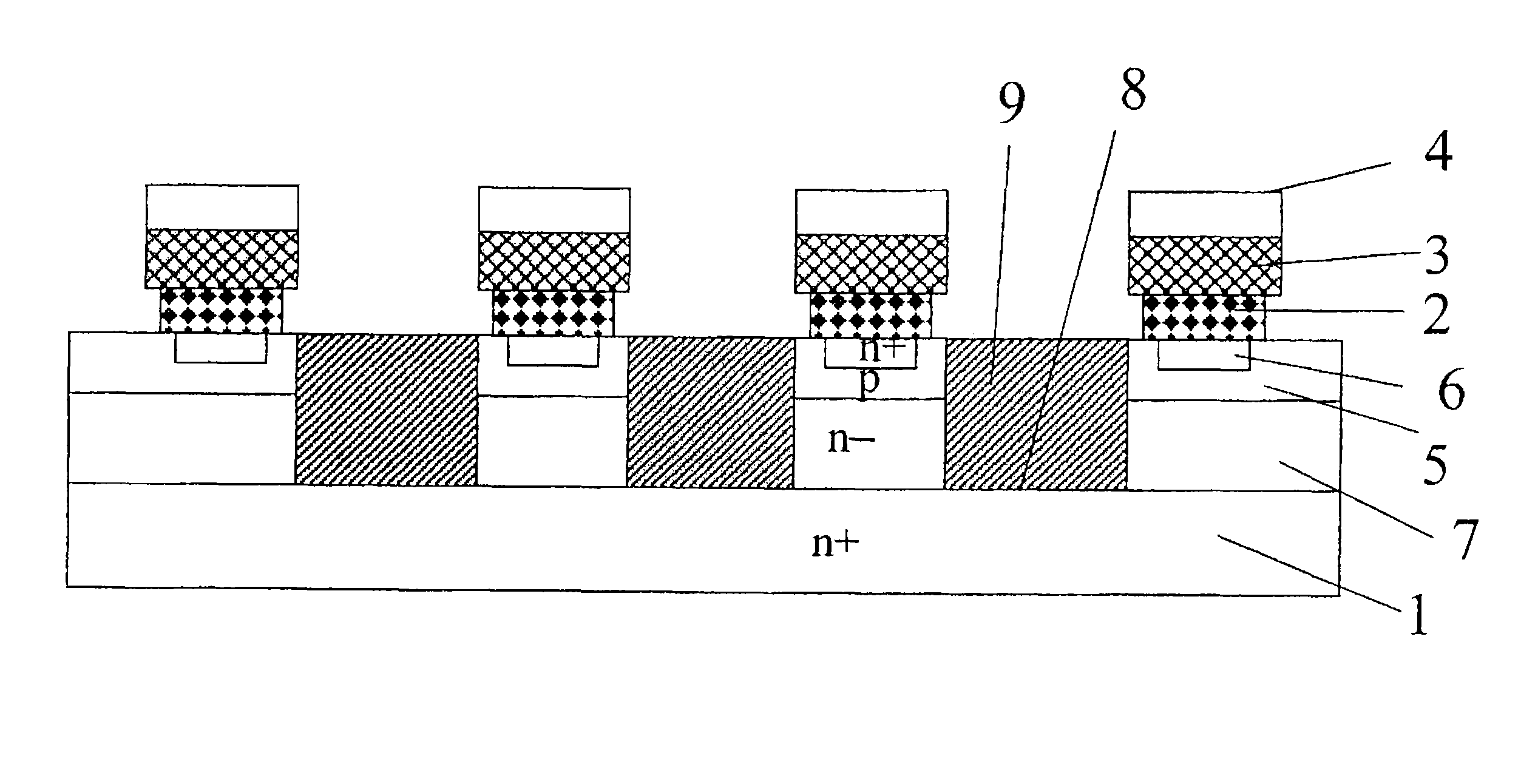
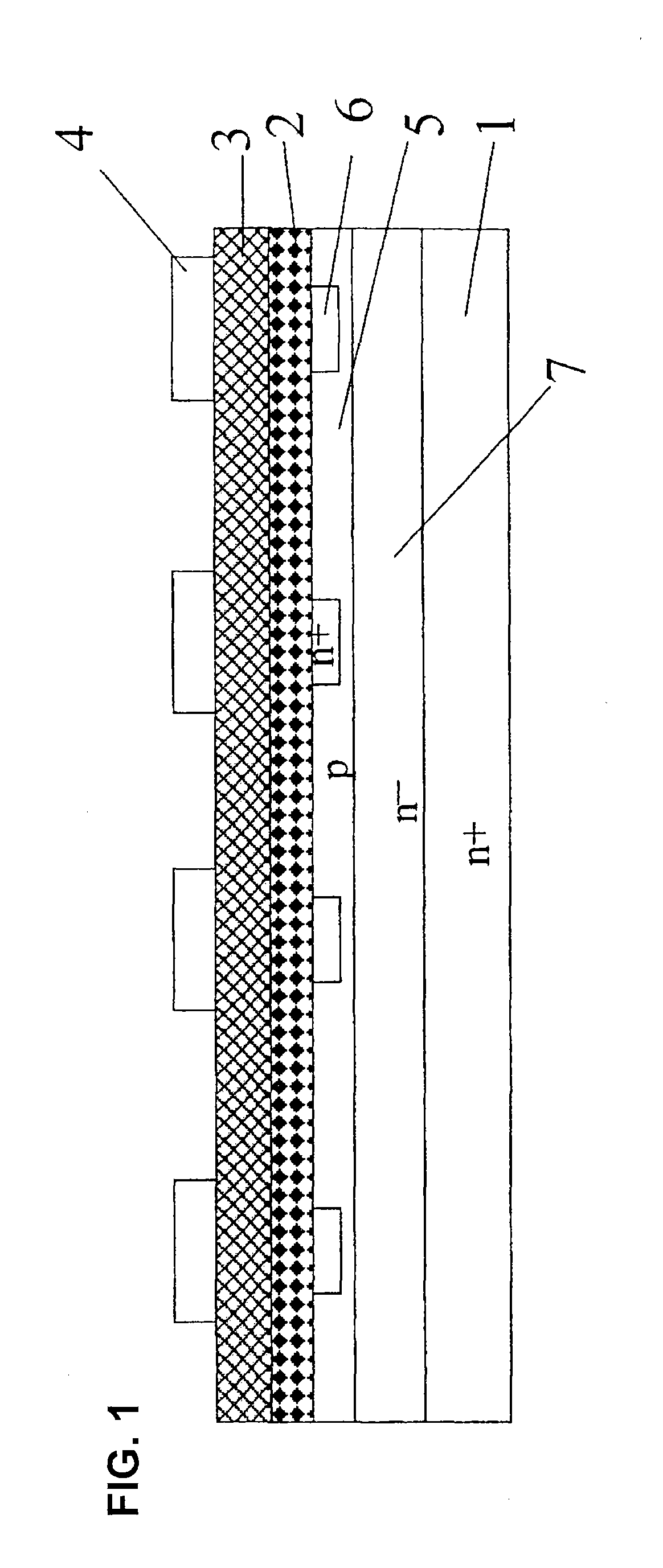
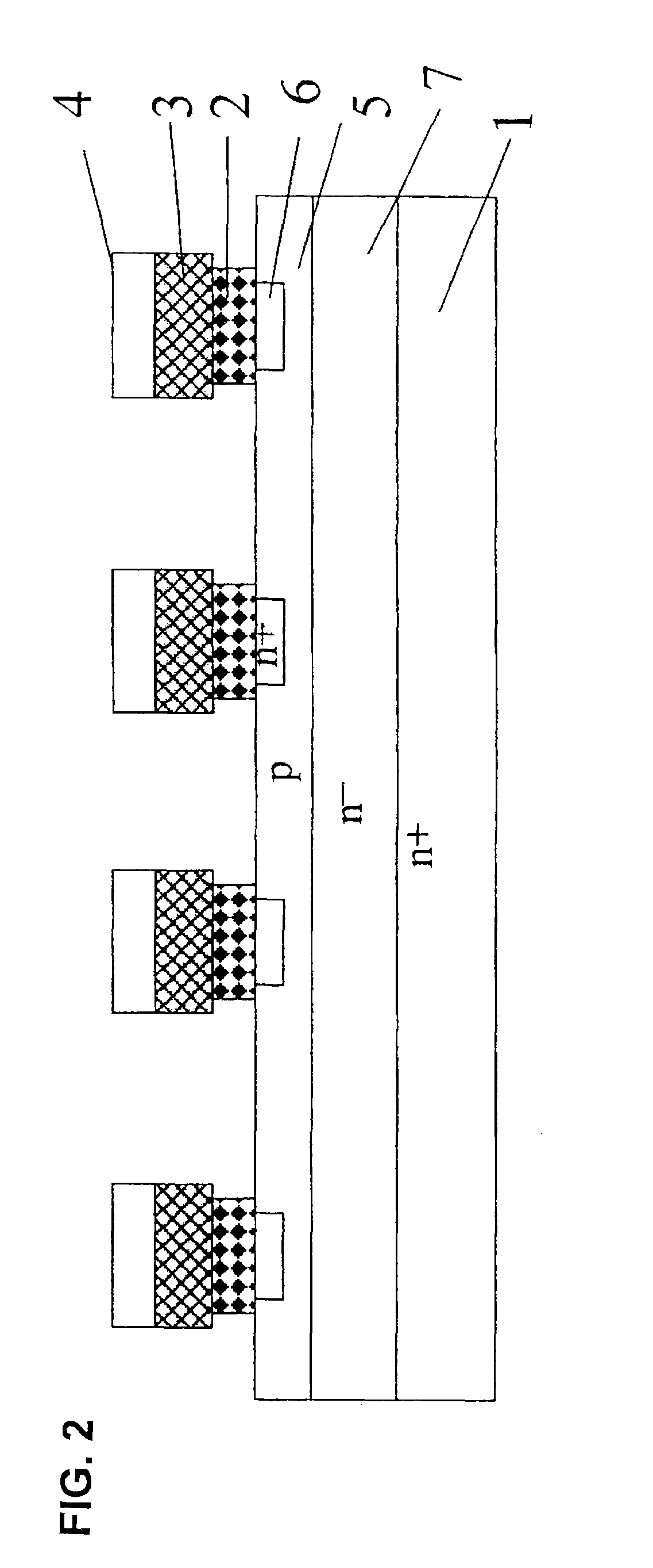
[0025]FIG. 1 is a sectional view of a silicon carbide wafer and shows a photoresist pattern. FIG. 2 is a sectional view of the silicon carbide wafer and shows a pattern of an etching mask which is a metal lamination film. FIGS. 3A through 3F are sectional views of silicon carbide wafers and shows respective etched shapes corresponding to Etching Condition 1 to Etching Condition 6, respectively. FIGS. 4A through 4C are sectional views of silicon carbide wafers which show respective etched shapes corresponding to Etching Condition 7 to Etching Condition 9, respectively. FIG. 5 is a sectional view of the silicon carbide wafer which is formed with mesa grooves.

[0026]As ...


PUM

PropertyMeasurementUnit
bias poweraaaaaaaaaa
total thicknessaaaaaaaaaa

Abstract

A manufacturing method for a silicon carbide semiconductor device is disclosed. It includes an etching method in which an Al film and Ni film are laid on an SiC wafer in this order and wet-etched, whereby a two-layer etching mask is formed in which Ni film portions overhang Al film portions. Mesa grooves are formed by dry etching by using this etching mask.

Description

CROSS REFERENCE TO RELATED APPLICATIONS[0001]This application claims priority from Japanese application Serial No. 2007-133597, filed on May 21, 2007, the contents of which are incorporated herein by reference in their entirety.BACKGROUND OF THE INVENTION[0002]A. Field of the Invention[0003]The present invention relates to a manufacturing method of a silicon carbide (hereinafter abbreviated as SiC) semiconductor device for high breakdown voltage and large current uses. More specifically, the invention relates to a manufacturing method including a dry etching method for forming a mesa groove having a junction end portion surface which surrounds an active portion where a main current flows in a power semiconductor device such as a diode or a MOSFET which uses a SiC semiconductor substrate.[0004]B. Description of the Related Art[0005]Power MOSFETs, IGBTs, etc. are known and widely used as silicon (hereinafter referred to as Si) power semiconductor devices which are used in inverters an...

Claims


Application Information

Patent Timeline
Patent Type & Authority Patents(United States)
IPC IPC(8): H01L21/3065H01L21/302
CPCH01L21/0475H01L29/0661Y10S438/931
Inventor KAWADA, YASUYUKI
Owner FUJI ELECTRIC CO LTD
Why Eureka
Try Eureka