Focus ring, plasma etching apparatus and plasma etching method

a plasma etching and focus ring technology, applied in the direction of adhesives, decorative arts, electric discharge tubes, etc., can solve the problems of increasing the connection between the source/drain of the cell transistor and the capacitor electrode, the need for deep trenches to be formed, and the difficulty of processing beyond the 0.18 m regim

Active Publication Date: 2009-10-15
TOKYO ELECTRON LTD
View PDF3 Cites 222 Cited by
  • Summary
  • Abstract
  • Description
  • Claims
  • Application Information

AI Technical Summary

Benefits of technology

[0013]The present invention is contrived on the basis of the aforementioned problems, and it is an object of the present invention to provide a focus ring, and a plasma etching apparatus and a method using the same, wherein reaction products are controlled to be properly deposited when performing a plasma etching on a substrate to form a recessed portion, e.g., a trench, thereby improving the etching performance.
[0014]The present invention has been developed on the basis of an examination result on a surface of a focus ring to find that, in case when performing a trench processing on a surface of a silicon wafer by a plasma etching, in-surface uniformity in an etching rate may be slightly changed with aging after the focus ring is replaced with a new one while an etching rate in the depth direction at an outer periphery of the silicon wafer is considerably lower than that in a central portion thereof, particularly, in the beginning of the use of the new one right after the replacement. Namely, while an inner surface of the focus ring is hardly consumed, an outer surface thereof is consumed significantly more compared to the inner surface, with aging. As described above, it has been considered that, if the surface of the focus ring is rough, reaction products are captured to be deposited thereonto and deposits thereof are detached therefrom, causing particle depositions on the side or the backside of the silicon wafer. However, it has been found out that individual parts of the surface should be considered. Namely, the outer periphery of the focus ring is highly consumed, and in such a state, the difference in the etching rates between the central part and the outer periphery part of the silicon wafer is small. This means that particle depositions onto the side or the backside of the silicon wafer are caused by deposits that are expected to be deposited on the inner surface of the focus ring; and the outer surface of the focus ring is rough, so that, if reaction products are captured to be deposited thereonto, they are prevented from being deposited on the outer periphery of the silicon wafer, thereby, suppressing a decrease in the etching rate in the corresponding outer periphery. The present invention is made on the basis of such an idea.

Problems solved by technology

On the other hand, it is disadvantageous in that a deeper trench needs to be formed to increase the storage capacitance since a high-K dielectric film cannot be used as a capacitor dielectric film.
Moreover, a connection between the source / drain of the cell transistor and a capacitor electrode is getting more difficult with the scaling down of the device; and particularly, a processing beyond a 0.18 μm regime becomes very difficult.
A conventional built-in power MOSFET formed on a surface of a silicon substrate utilizes only an extremely small area on the surface of the substrate to thereby put a limitation in reducing an electrode gap since a high voltage applied thereto needs to be controlled, resulting in hampering the lowering of the on-resistance.
However, since the single crystalline has no base layer to stop etching, if an etching rate in a central part of the wafer is different from that in an outer periphery thereof (outer margin), in-surface uniformity of the wafer along the depth of the trench becomes deteriorated.

Method used


Image

  • Focus ring, plasma etching apparatus and plasma etching method
  • Focus ring, plasma etching apparatus and plasma etching method
  • Focus ring, plasma etching apparatus and plasma etching method

Examples


Embodiment Construction

[0028]Hereinafter, preferred embodiments of the present invention will be described in detail with reference to the accompanying drawings.

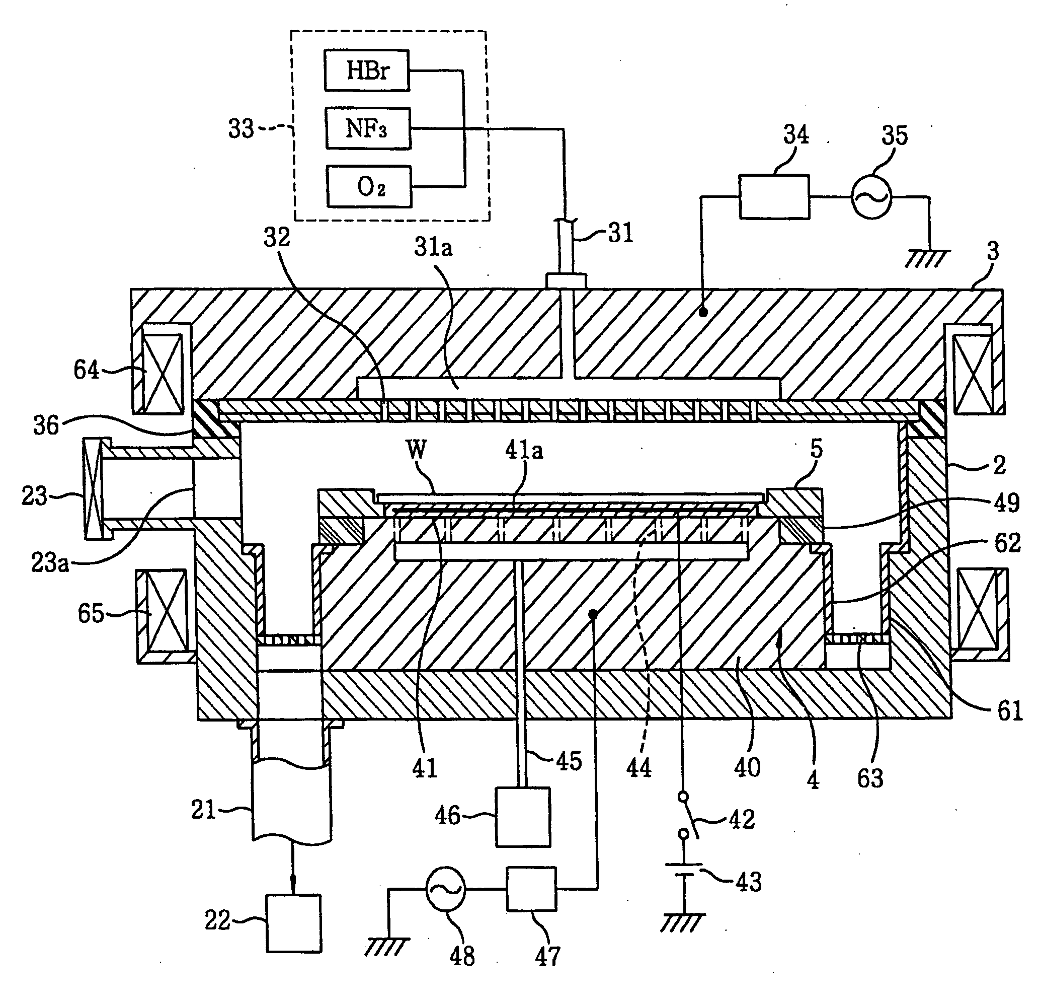
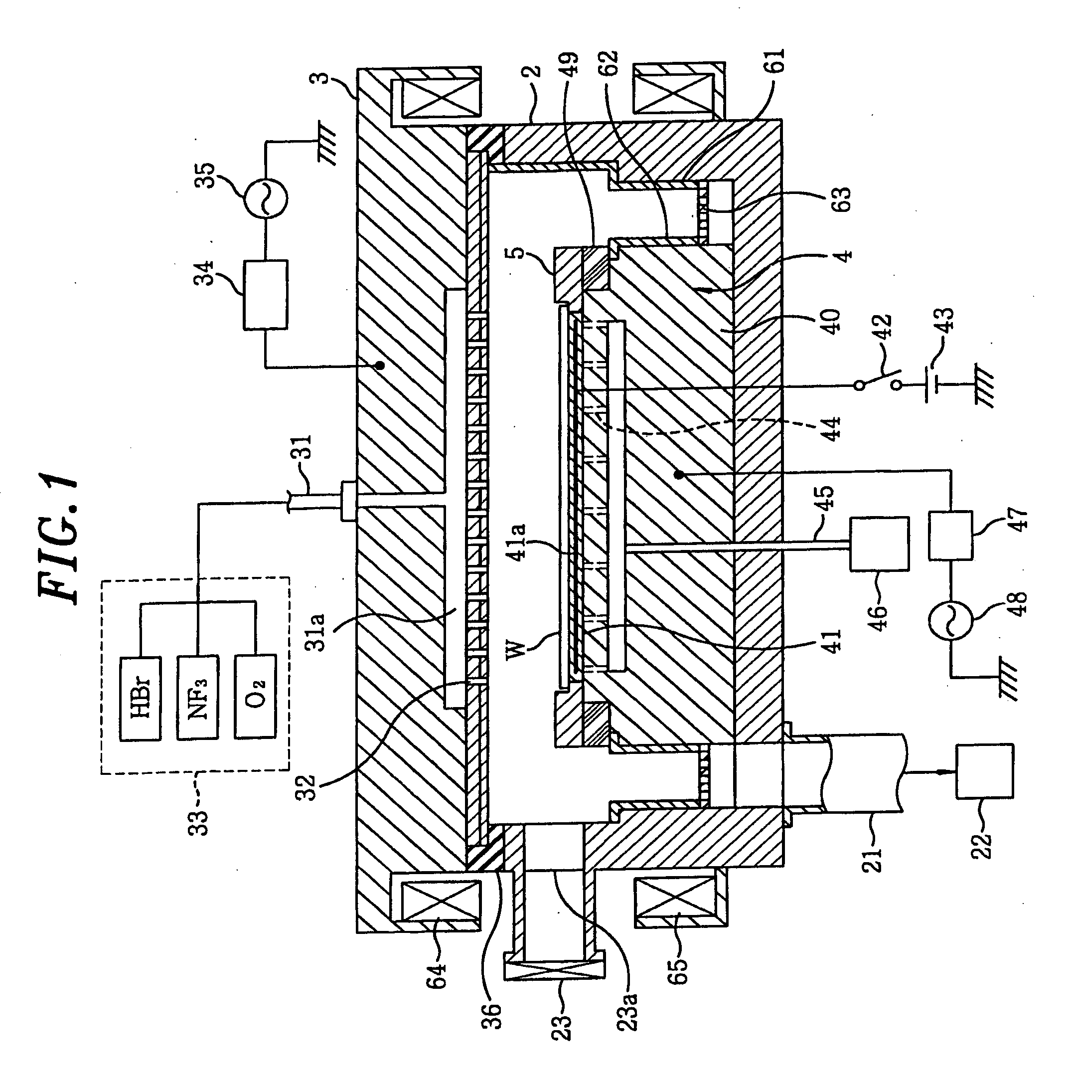
[0029]As a preferred embodiment of a plasma etching apparatus using a focus ring in accordance with the present invention, a magnetron reactive ion etching apparatus will now be explained as an example. Reference numeral 2 in the drawing indicates an airtight processing vessel made of a conductive member, e.g., aluminum, which is grounded. Further, the processing vessel 2 has an upper electrode 3 also serving as a gas shower head of a gas supply unit for introducing a processing gas for performing an etching; and a susceptor 4, also serving as a lower electrode, for mounting thereon a substrate, e.g., a silicon wafer (hereinafter, referred to as a wafer) W, the upper electrode 3 and the susceptor 4 being arranged to face each other.

[0030]Still further, a gas exhaust line 21, coupled to a bottom portion of the processing vessel 2, is coupled at the...


PUM

PropertyMeasurementUnit
surface roughness Raaaaaaaaaaa
surface roughnessaaaaaaaaaa

Abstract

In a plasma etching apparatus for performing a plasma etching on a surface of a substrate mounted on a susceptor in a processing vessel, a focus ring is installed to surround the substrate and has a first region at an inner side on a surface thereof, in which an average surface roughness is small such that a reaction product produced during an etching processing is not captured to be deposited, and a second region at an outer side from the first region, in which an average surface roughness is large such that a reaction product produced during the etching process is captured to be deposited. A boundary between the first and the second region is a part where an etching amount is relatively significantly changed compared to other parts while the focus ring is equipped in the plasma etching apparatus and the plasma etching is performed on the substrate.

Description

CROSS-REFERENCE TO RELATED APPLICATIONS[0001]This application is a continuation of U.S. application Ser. No. 11 / 270,461 filed Nov. 10, 2005, the entire contents of which is incorporated herein by reference. U.S. application Ser. No. 11 / 270,461 claims the benefit of priority under 119(e) of U.S. Provisional Application No. 60 / 635,613, filed Dec. 14, 2004, and claims the benefit of priority under 35 U.S.C. §119 from Japanese Patent Application Number 2004-331071, filed Nov. 15, 2004.FIELD OF THE INVENTION[0002]The present invention relates to a focus ring, a plasma etching apparatus and a plasma etching method, wherein the focus ring is used in the plasma etching apparatus for performing an etching by using a plasma on a substrate, e.g., a semiconductor wafer, and forming, e.g., a trench on a surface of the substrate.BACKGROUND OF THE INVENTION[0003]A logic embedded DRAM has begun to expand its significant commercial applications into the field of digital appliances such as a digital ...

Claims


Application Information

Patent Timeline
Patent Type & Authority Applications(United States)
IPC IPC(8): B44C1/22C23F1/08
CPCH01L21/67069H01J37/32642Y10S156/915
Inventor SATOH, DAIKIKOBAYASHI, HIDEYUKIHORIGUCHI, MASATO
Owner TOKYO ELECTRON LTD
Why Eureka
Try Eureka