Semiconductor device and method of fabricating the same

a technology of semiconductors and fins, applied in the direction of semiconductor devices, electrical equipment, transistors, etc., can solve the problems that the layout design of fins still faces some issues in conventional fins fabrication, and achieve the effects of improving the etching effect of fins, preventing collapsing or overetching, and improving isolation

Active Publication Date: 2017-03-30
UNITED MICROELECTRONICS CORP
View PDF0 Cites 24 Cited by
  • Summary
  • Abstract
  • Description
  • Claims
  • Application Information

AI Technical Summary

Benefits of technology

[0009]According to these, the semiconductor device and the forming method thereof in the present invention mainly forms a trench lower than the shallow trench isolation through a multi-stepped fin cut process, wherein the trench has a depth being smaller than a width of each of the fin shaped structures. Through forming such trench, the present invention enables to provide better isolation without causing any disturbance to the element formed subsequently. Also, since the trench is formed by progressively removing the dummy fin shaped structures and the organic dielectric layer filled therebetween, the present invention also enables to improve the etching effect of the fin shaped structures, and to keep from collapsing or over-etching issues during the fin cutting process.

Problems solved by technology

However, layout designs of the FinFET structures still face some issues in conventional FinFET fabrication.

Method used


Image

  • Semiconductor device and method of fabricating the same
  • Semiconductor device and method of fabricating the same
  • Semiconductor device and method of fabricating the same

Examples


Embodiment Construction

[0013]To provide a better understanding of the present invention, preferred embodiments will be described in detail. The preferred embodiments of the present invention are illustrated in the accompanying drawings with numbered elements.

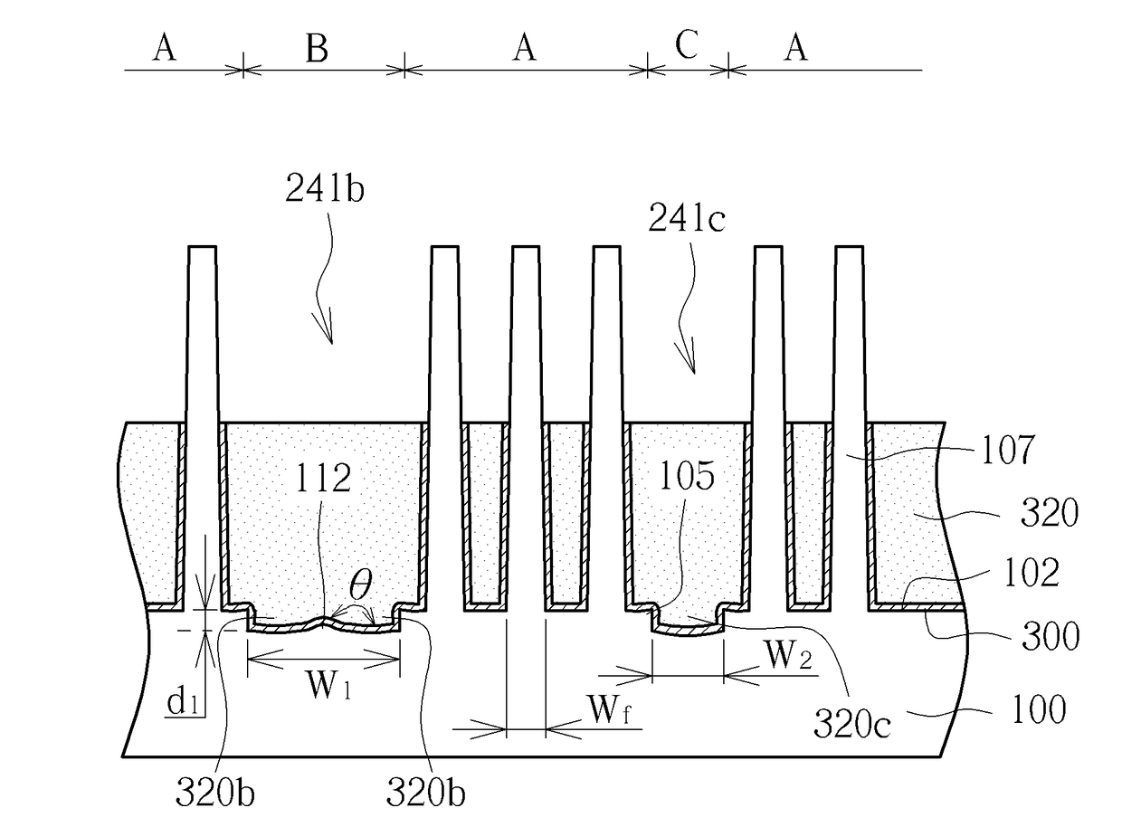
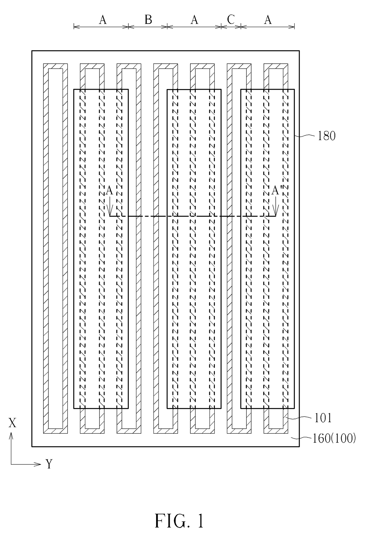
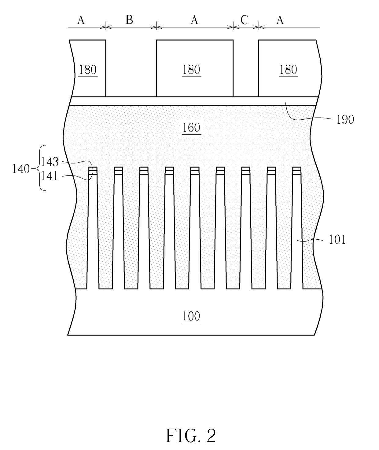
[0014]Please refer to FIG. 1 to FIG. 4, which are schematic diagrams illustrating a method of forming a semiconductor device according to the first embodiment of the present invention, wherein FIG. 1 shows top views of the semiconductor device in forming steps, and FIGS. 2-4 show cross-sectional views of the semiconductor device in forming steps taken along a cross line A-A′ in FIG. 1. First of all, a substrate 100 is provided and plural regions A, B, C are defined on the substrate 100. The substrate 100 may include a semiconductor substrate, like a silicon substrate a silicon-containing substrate or a silicon-on-insulator (SOI) substrate for example, and a plurality of fin shaped structures 101 is formed on a base 102 of the substrate 100.

[0015]In on...


PUM


Abstract

A semiconductor device and a method of fabricating the same, the semiconductor device includes a substrate, a plurality of fin shaped structures, a first trench and at least one bump. The substrate has a base. The fin shaped structures protrude from the base of the substrate. The first trench recesses from the base of the substrate and has a depth being smaller than a width of each of the fin shaped structures. The at least one bump is disposed on a surface of the first trench.

Description

BACKGROUND OF THE INVENTION[0001]1. Field of the Invention[0002]The invention relates to a semiconductor device and a method of forming the same, and more particularly, to a semiconductor device having fin shaped structures and a method of forming the same.[0003]2. Description of the Prior Art[0004]With the trend in the industry being scaling down the size of the field effect transistors (FETs), three-dimensional or non-planar transistor technology, such as fin field effect transistor technology (FinFET) has been developed to replace planar FETs. Since the three-dimensional structure of a FinFET increases the overlapping area between the gate and the fin-shaped structure of the silicon substrate, the channel region can therefore be more effectively controlled. This way, the drain-induced barrier lowering (DIBL) effect and the short channel effect are reduced. The channel region is also longer for an equivalent gate length, thus the current between the source and the drain is increas...

Claims


Application Information

Patent Timeline
Patent Type & Authority Applications(United States)
IPC IPC(8): H01L27/088H01L21/02H01L21/306H01L21/762H01L21/8234H01L29/06H01L21/3105
CPCH01L27/0886H01L29/0653H01L21/02118H01L21/30604H01L21/76224H01L21/823431H01L21/823481H01L21/31058H01L21/3081H01L21/762
Inventor TSENG, I-MINGLIANG, WEN-ANHUANG, CHEN-MING
Owner UNITED MICROELECTRONICS CORP
Why Eureka
Try Eureka