Electronic component package and method of manufacturing the same

a technology of electronic components and components, applied in the direction of printed circuit non-printed electric components association, semiconductor/solid-state device details, non-metallic protective coating applications, etc., can solve the problem and achieve the effect of reducing the yield of electronic components

Active Publication Date: 2016-11-17
SAMSUNG ELECTRONICS CO LTD
View PDF11 Cites 123 Cited by
  • Summary
  • Abstract
  • Description
  • Claims
  • Application Information

AI Technical Summary

Benefits of technology

[0008]An aspect of the present disclosure may provide an electronic component package in which a problem that a yield of an electronic component is decreased may be solved, a method of manufacturing the same, and a package-on-package structure.

Problems solved by technology

In this case, a defect occurring in processes after the electronic component is disposed causes a decrease in a yield of the electronic component.

Method used


Image

  • Electronic component package and method of manufacturing the same
  • Electronic component package and method of manufacturing the same
  • Electronic component package and method of manufacturing the same

Examples


Embodiment Construction

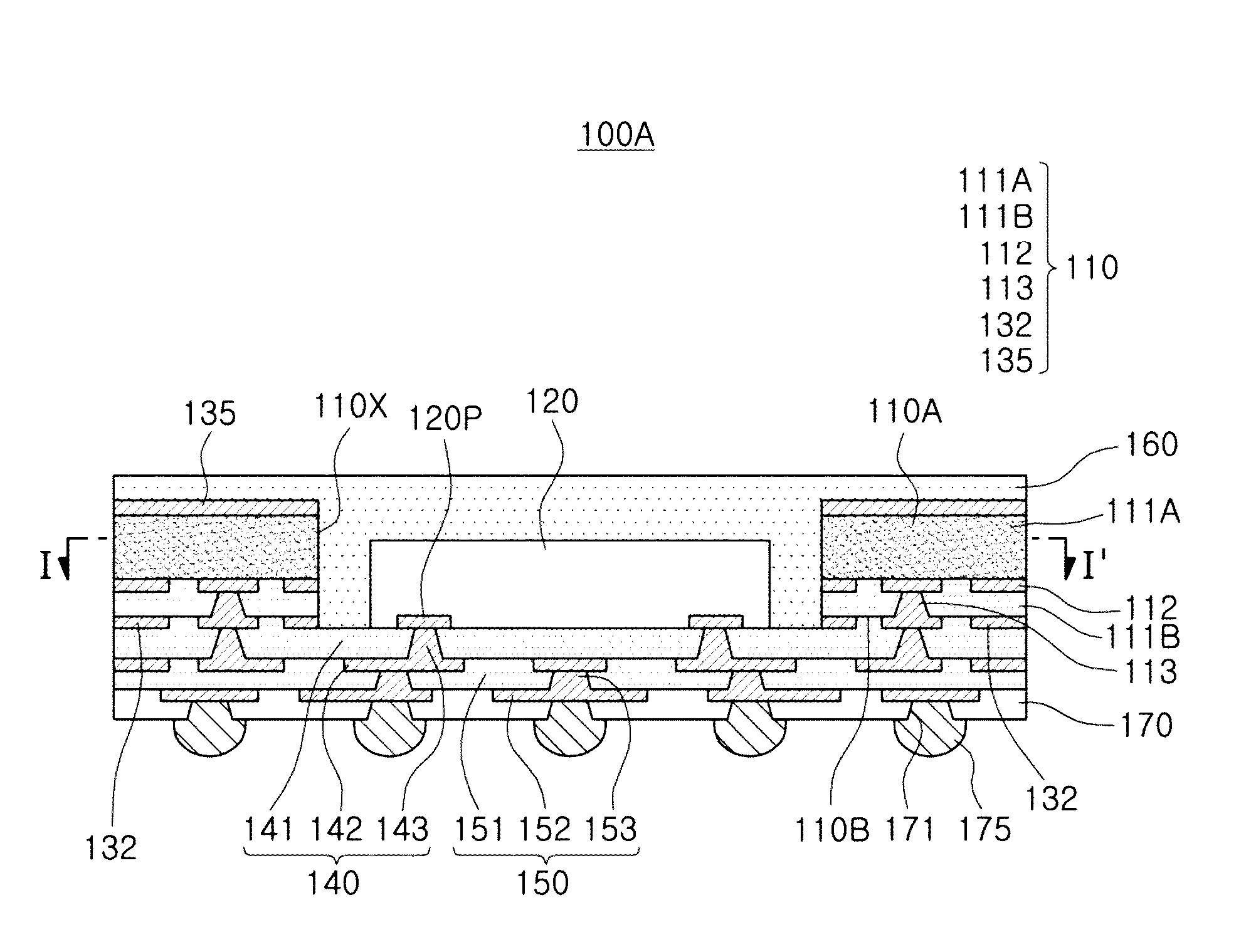
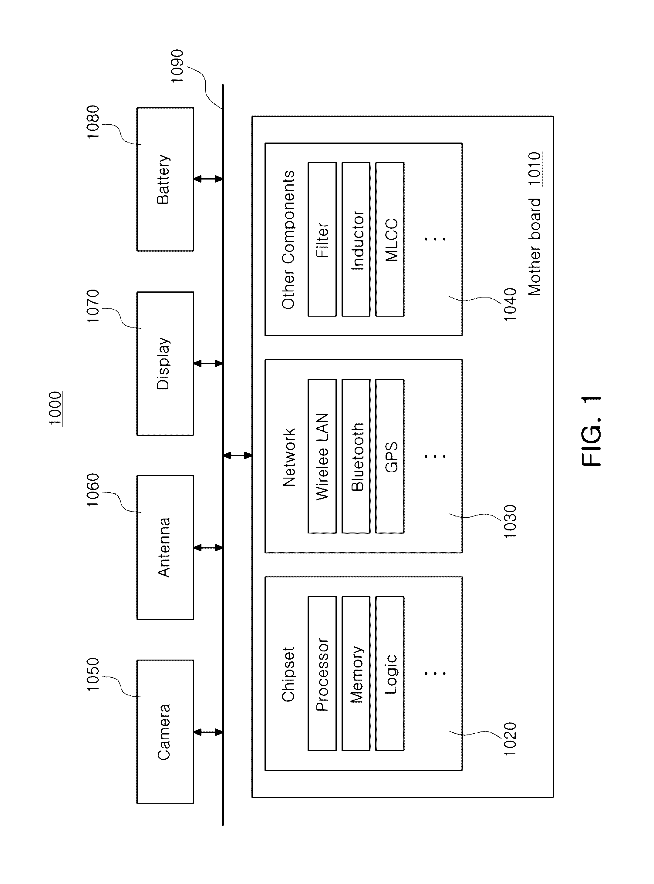
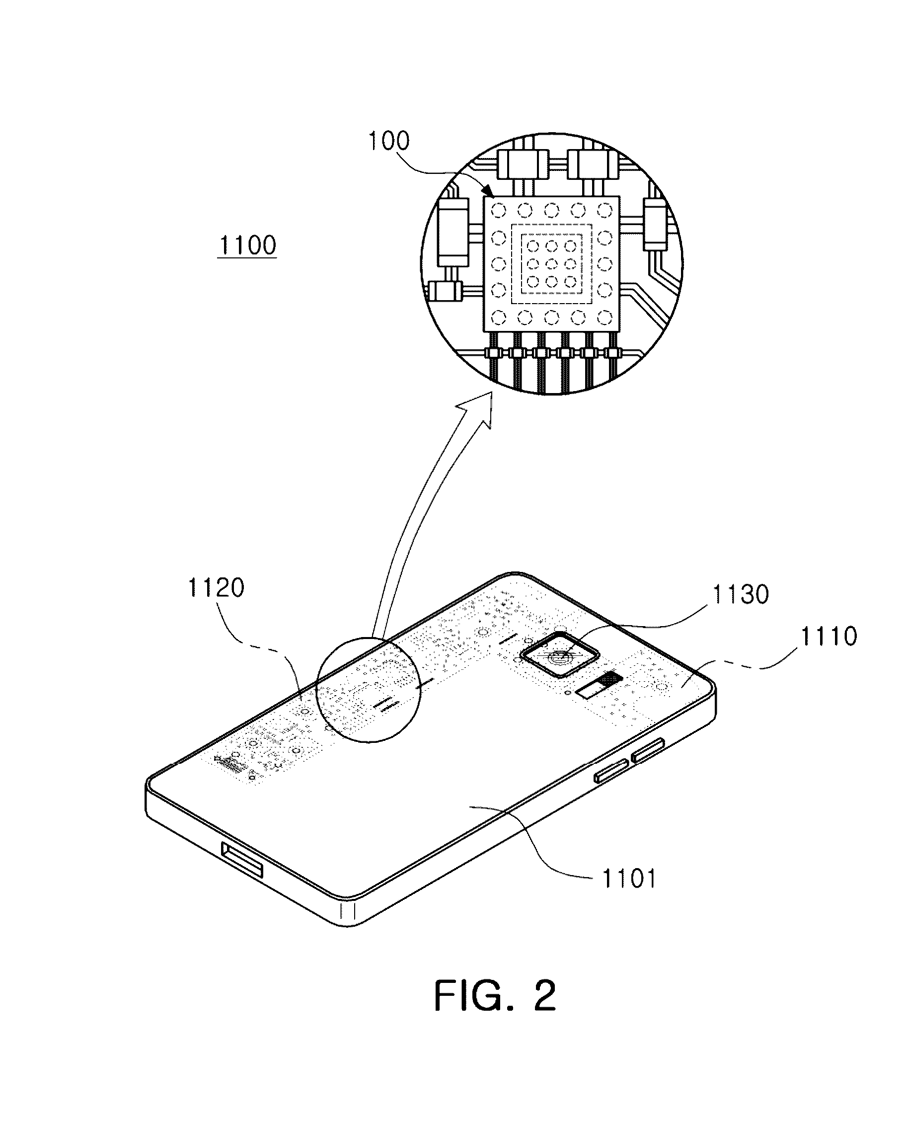
[0059]Hereinafter, embodiments of the present disclosure will be described as follows with reference to the attached drawings.

[0060]The present disclosure may, however, be exemplified in many different forms and should not be construed as being limited to the specific embodiments set forth herein. Rather, these embodiments are provided so that this disclosure will be thorough and complete, and will fully convey the scope of the disclosure to those skilled in the art.

[0061]Throughout the specification, it will be understood that when an element, such as a layer, region or wafer (substrate), is referred to as being “on,”“connected to,” or “coupled to” another element, it can be directly “on,”“connected to,” or “coupled to” the other element or other elements intervening therebetween may be present. In contrast, when an element is referred to as being “directly on,”“directly connected to,” or “directly coupled to” another element, there may be no elements or layers intervening therebet...


PUM


Abstract

An electronic component package and a method of manufacturing the same are provided. The electronic component package includes a frame having a through-hole, an electronic component disposed in the through-hole of the frame, and a redistribution part disposed at one side of the frame and the electronic component. One or more first wiring layers of the frame are electrically connected to the electronic component through the redistribution part.

Description

CROSS-REFERENCE TO RELATED APPLICATIONS[0001]This application claims benefits of priorities to Korean Patent Application Nos. 10-2015-0065177 filed on May 11, 2015, 10-2015-0139682 filed on Oct. 5, 2015, and 10-2016-0047455 filed on Apr. 19, 2016, with the Korean Intellectual Property Office, the disclosures of which are incorporated herein by reference.BACKGROUND[0002]1. Field[0003]The present disclosure relates to an electronic component package and a method of manufacturing the same.[0004]2. Description of Related Art[0005]An electronic component package is defined as package technology for electrically connecting an electronic component to a printed circuit board (PCB), such as a main board of an electronic device, or the like, and protecting the electronic component from external impact, and is distinguished from an embedded technology of embedding an electronic component in a printed circuit board, such as an interposer substrate. Meanwhile, one of the main recent trends withi...

Claims


Application Information

Patent Timeline
Patent Type & Authority Applications(United States)
IPC IPC(8): H05K1/18H05K3/28H05K1/02H05K3/30
CPCH05K1/184H05K1/0298H05K3/284H05K3/306H05K1/0271H05K1/185H05K2201/10674H01L24/19H01L21/568H01L2224/04105H01L2224/12105H01L2224/16227H01L2224/24195H01L2224/32145H01L2224/32225H01L2224/48091H01L2224/48227H01L2224/73204H01L2224/73253H01L2224/73265H01L2225/0651H01L2225/06517H01L2225/1035H01L2225/1041H01L2225/1058H01L2924/15311H01L2924/19105H01L2225/06558H01L2924/181H01L2924/00014H01L2924/3025H01L2924/3511H01L23/49816H01L23/50H01L23/5389H01L2224/18H01L2924/00012H01L2924/00H01L2224/45099H01L2924/0001H01L2224/16225H01L23/48H01L24/00
Inventor PARK, DAE HYUNKIM, HANHUR, KANG HEONKO, YOUNG GWANSHIM, JUNG HO
Owner SAMSUNG ELECTRONICS CO LTD
Why Eureka
Try Eureka