Light emitting diode chip with double close-loop electrode design

a technology of light-emitting diodes and electrodes, which is applied in the direction of basic electric elements, electrical equipment, and semiconductor devices, can solve the problems of reducing the luminous efficiency of led chips b>100/b>, and achieve the effects of improving light radiation, reducing luminous efficiency, and improving luminous efficiency

Inactive Publication Date: 2007-08-30
EPISTAR CORP
View PDF6 Cites 12 Cited by
  • Summary
  • Abstract
  • Description
  • Claims
  • Application Information

AI Technical Summary

Benefits of technology

[0022] In summary, in the LED chip with double close-loop electrode design of the present invention, since both the first electrode and the second electrode have close-loop patterns, if the first electrode or the second electrode is broken, the electrodes at both ends of the broken area still remain electric conductivity without affecting the luminous efficiency of the LED chip. Besides, since the hollow region inside the profile of the second electrode in the present invention goes through the second-type doped semiconductor layer and the light emitting layer for exposing the first-type doped semiconductor layer, the light radiation can be improved and the luminous efficiency can be upgraded.

Problems solved by technology

Consequently, a partial region of the light emitting layer 130 would not radiate light, which reduces the luminous efficiency of the LED chip 100.

Method used


Image

  • Light emitting diode chip with double close-loop electrode design
  • Light emitting diode chip with double close-loop electrode design
  • Light emitting diode chip with double close-loop electrode design

Examples


first embodiment

The First Embodiment

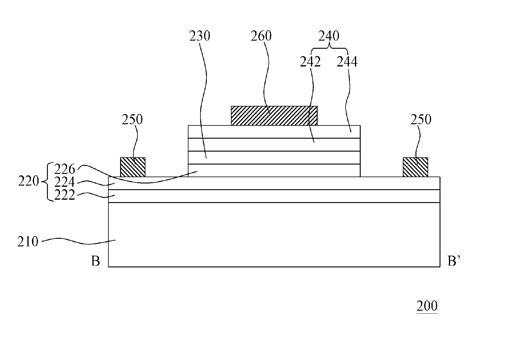
[0032]FIG. 2A is a diagram of an LED chip with double closed-loop electrode design according to the first embodiment of the present invention and FIG. 2B is a schematic cross-sectional drawing taken along section plane B-B′ in FIG. 2A. Referring to FIGS. 2A and 2B, an LED chip 200 with double close-loop electrode design of the present invention includes a substrate 210, a first-type doped semiconductor layer 220, a light emitting layer 230, a second-type doped semiconductor layer 240, a first electrode 250 and a second electrode 260. The first-type doped semiconductor layer 220 is disposed on the substrate 210; the light emitting layer 230 is disposed on the first-type doped semiconductor layer 220 and exposes a part of the first-type doped semiconductor layer 220, while the second-type doped semiconductor layer 240 is disposed on the light emitting layer 230. The first electrode 250 is disposed on the first-type doped semiconductor layer 220 and has a close-loop...

second embodiment

The Second Embodiment

[0043]FIG. 3 is a schematic top view of an LED chip with double closed-loop electrode design according to the second embodiment of the present invention. Referring to FIG. 3, the LED chip 300 with double close-loop electrode design of the present embodiment is similar to the LED chip 200 with double close-loop electrode design in the first embodiment (shown in FIG. 2A) except for the following unique points described in detail. In the embodiment, a first electrode 250 includes a close-loop pattern 252 and a plurality of first branches 254. The close-loop pattern 252 is an encircled close region S on the first-type doped semiconductor layer 220, while the first branches 254 are connected to the close-loop pattern 252 and located inside the close region S. Besides, a second electrode 260 can include a plurality of second branches 262. The first branches 254 and the second branches 262 are alternately arranged. In this way, the distance between the first electrode ...

third embodiment

The Third Embodiment

[0045]FIG. 4A is a schematic top view of an LED chip with double closed-loop electrode design according to the third embodiment of the present invention and FIG. 4B is a schematic cross-sectional drawing taken along section plane D-D′ in FIG. 4A. Referring to FIGS. 4A and 4B, the LED chip 400 with double close-loop electrode design of the present embodiment is similar to the LED chip 300 with double close-loop electrode design in the second embodiment (shown in FIG. 3) except that partial regions inside the profiles of the first branches 254 in the LED chip 400 with double close-loop electrode design are a plurality of hollow regions 290. Besides, on the exposed surfaces of the first-type doped semiconductor layer 220 in the LED chip 400 with double close-loop electrode design, a micro-structure 280 is formed.

[0046] Additionally, since the hollow regions 290 are the partial regions inside the profiles of the first branches 254, the close-loop pattern 252 and the...


PUM


Abstract

An LED chip with double close-loop electrode design includes a substrate, a first-type doped semiconductor layer, a light emitting layer, a second-type doped semiconductor layer, a first electrode and a second electrode. The first-type doped semiconductor layer is disposed on the substrate, the light emitting layer is disposed on the first-type doped semiconductor layer and the second-type doped semiconductor layer is disposed on the light emitting layer. The first electrode, disposed on the first-type doped semiconductor layer, has a close-loop pattern. The second electrode, disposed on the second-type doped semiconductor layer, is located inside a region encircled by the first electrode and has a close-loop pattern. In this way, the LED chip with double close-loop electrode design is able to avoid deteriorated luminous efficiency caused by broken electrodes.

Description

BACKGROUND OF THE INVENTION [0001] 1. Field of Invention [0002] The present invention relates to a semiconductor device, and particularly to a light emitting diode chip (LED chip). [0003] 2. Description of the Related Art [0004] A light emitting diode (LED) is a semiconductor device, and the material of the emitting chip is usually chemical elements of group III, group IV and group V, namely compound semiconductors, such as gallium phosphide (GaP), gallium arsenide (GaAs) and gallium nitride (GaN). Applying current to the compound semiconductors by means of recombination of electrons and holes, the electric energy is converted into optic energy and released in photon form to achieve light radiation. The light radiation of an LED is belonged to the so-called “cool light radiation”, rather than radiated by heat, therefore, the lifetime of an LED can be over a hundred thousand hours without any idling time. In addition, an LED has advantages such as fast response speed (about 10-9 seco...

Claims


Application Information

Patent Timeline
Patent Type & Authority Applications(United States)
IPC IPC(8): H01L33/00H01L33/22H01L33/38
CPCH01L33/20H01L33/38H01L33/22
Inventor LI, YUN-LIFENG, HUI-CHING
Owner EPISTAR CORP
Why Eureka
Try Eureka