

Input device and I/O-integrated display
- Summary
- Abstract
- Description
- Claims
- Application Information
AI Technical Summary
Benefits of technology
Problems solved by technology
Method used
Image

Examples
embodiment 1
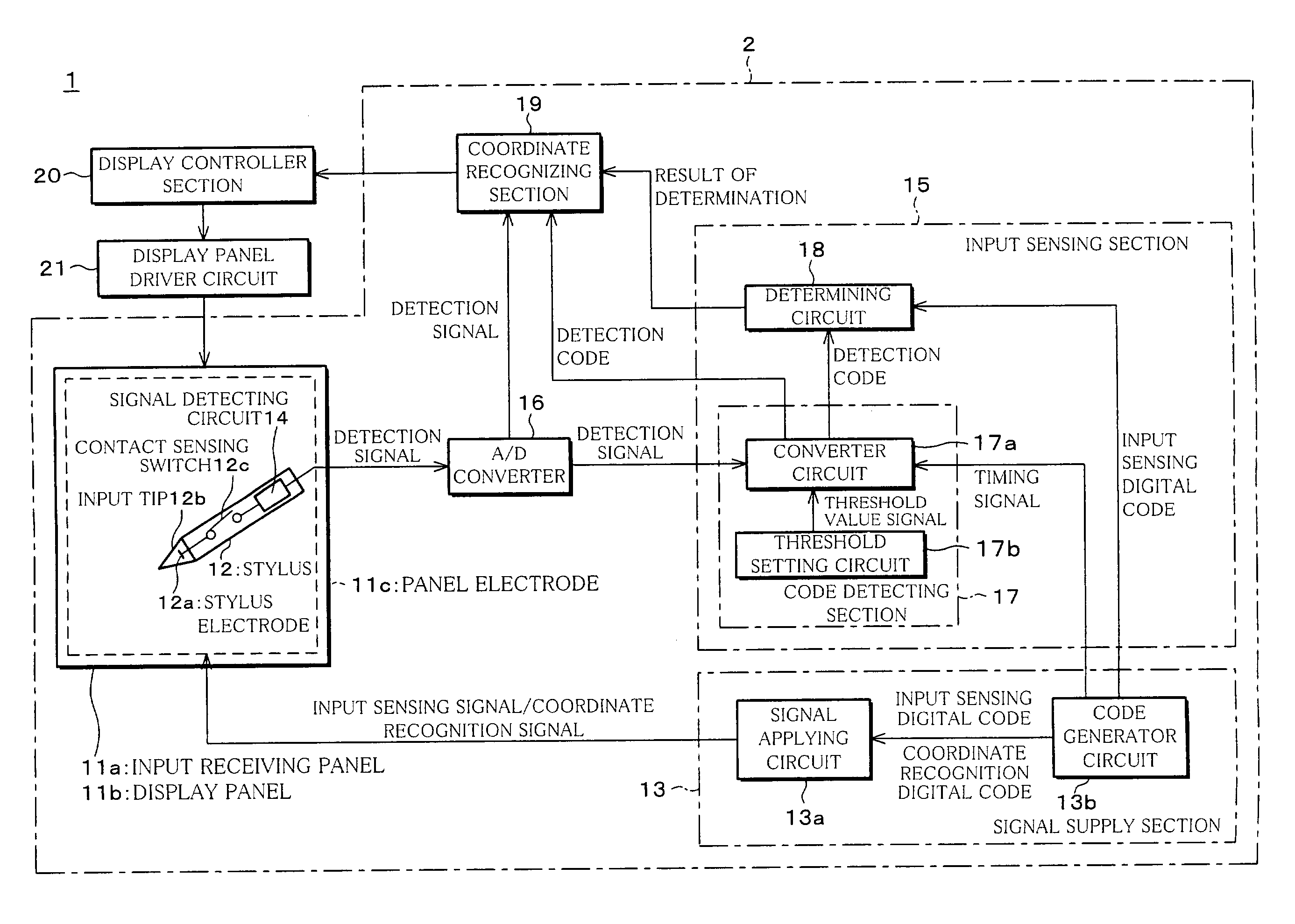
[0097]The I / O-integrated display 1 in FIG. 1 with the input device 2 is now discussed. In embodiment 1, the display is a so-called “opposite source, active matrix liquid crystal display.” The display panel 50 as the display panel 11b in FIG. 1 is arranged as shown in FIG. 9 and FIG. 10. FIG. 10 is an equivalent circuit of the display panel 50. The display panel 50 includes a first, active matrix substrate 55 and a second, opposite substrate 57.
[0098]On the first substrate 55 are there formed a matrix of pixel electrodes 51 arranged in rows and columns, a plurality of TFTs (switching elements) 52 each provided to a different pixel electrode 51, a plurality of scan lines 53 each provided in a different row and connected to all the gates (control leads) of those TFTs 52 which sit in that row, and a plurality of reference lines 54 each provided in a different row and connected to all those pixel electrodes 51 which sit in that row through those associated TFTs 52. The reference lines 54...
embodiment 2
[0120]The I / O-integrated display 1 in FIG. 1 with the input device 2 is now discussed. In embodiment 2, the display is a so-called “opposite common electrode, active matrix liquid crystal display.” The display panel 70 as the display panel 11b in FIG. 1 is arranged as shown in FIG. 14 and FIG. 15. FIG. 15 is an equivalent circuit of the display panel 70. Those components in FIG. 14 and FIG. 15 which have equivalent functions as those in FIG. 9 and FIG. 10 are identified by the same numerals as in FIG. 9 and FIG. 10. The display panel 70 includes a first, active matrix substrate 55 and a second, opposite substrate 57 too. The display panel 70 has following differences from the display panel 50.
[0121]On the first substrate 55 are there formed a plurality of signal lines 76 each provided in a different column and connected to all those pixel electrodes 51 which sit in that column through those associated TFTs 52. That is, the signal lines 76 are arranged to cross the scan lines 53. The...
PUM
 Abstract
Description
Claims
Application Information