

Connection structure of flexible substrate
a technology of flexible substrates and connections, applied in the direction of insulated conductors, cables, magnetic bodies, etc., can solve the problems of increasing the outside dimension of figures, increasing the cost of figures, etc., and achieve the effect of reducing the outside dimension of the counterpart substrate 1 and forming easily
- Summary
- Abstract
- Description
- Claims
- Application Information
AI Technical Summary
Benefits of technology
Problems solved by technology
Method used
Image

Examples
Embodiment Construction
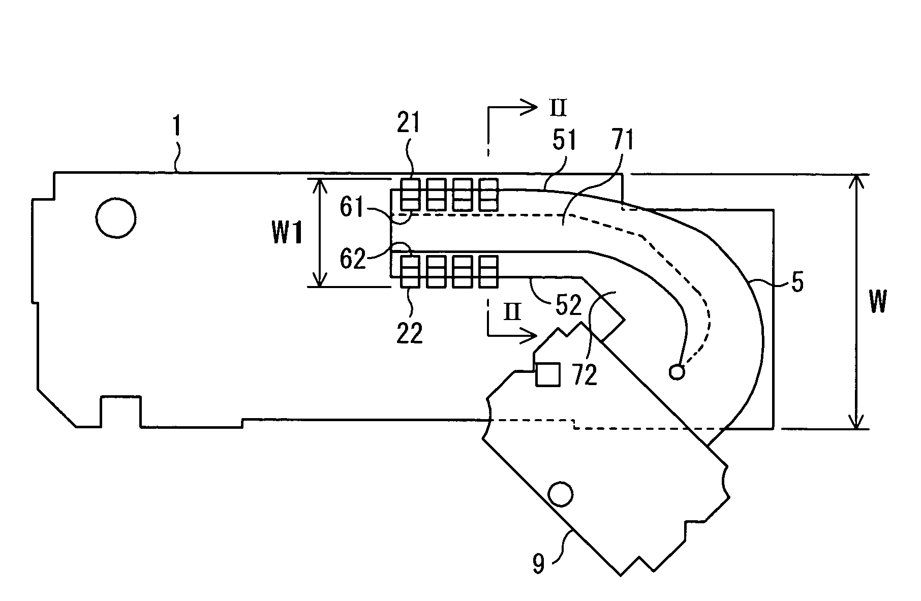
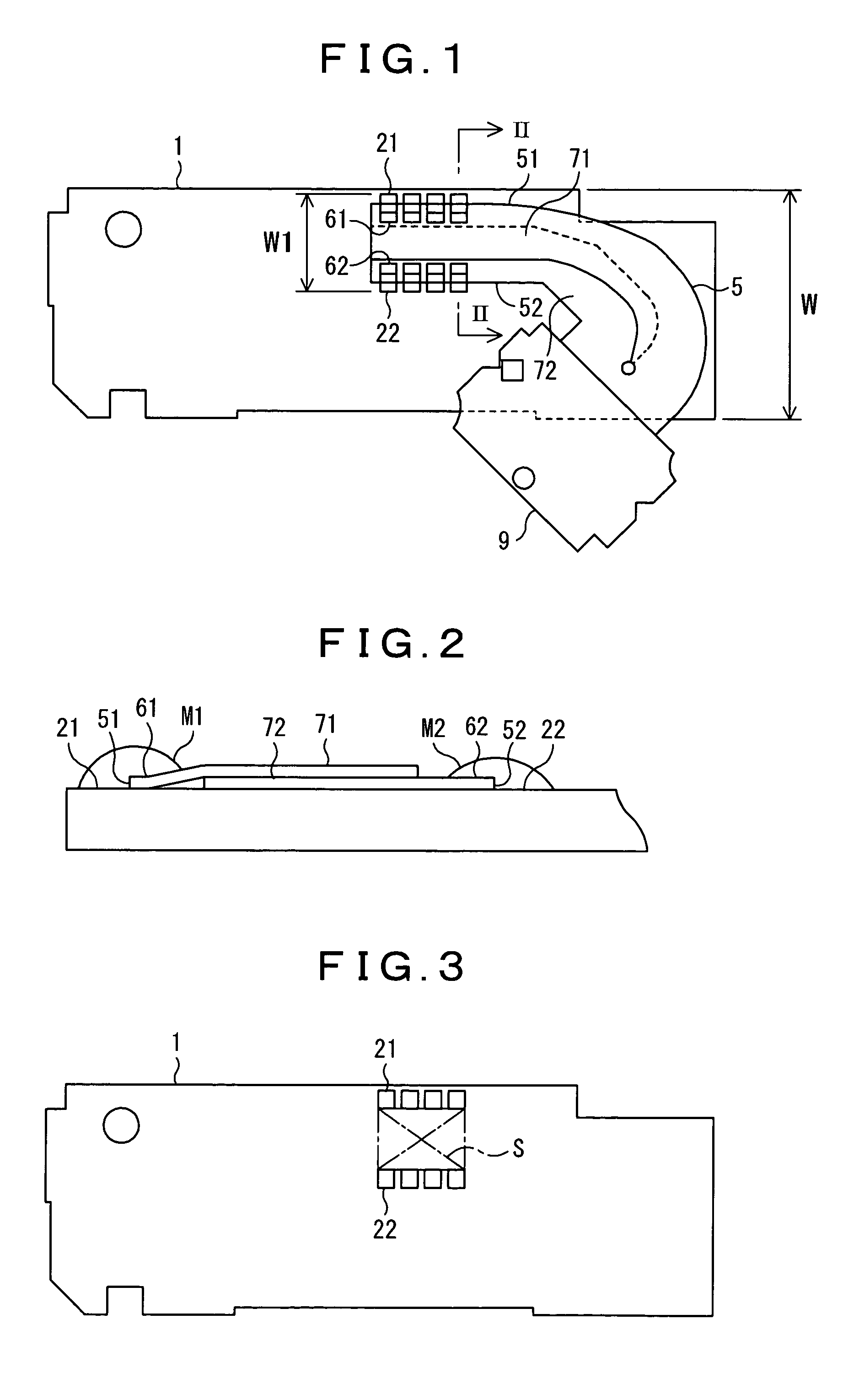
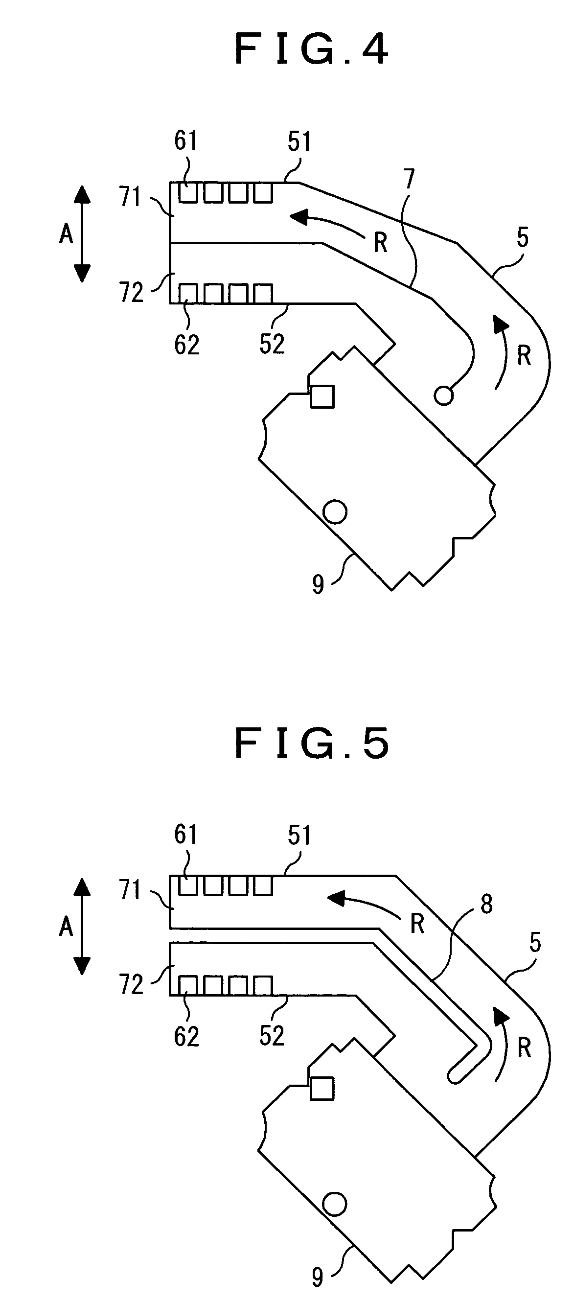
[0031]FIG. 1 is a plan view of a connection structure of a flexible substrate according to an embodiment, and FIG. 2 is an illustrative enlarged cross-sectional view along the arrows II-II in FIG. 1. Further, FIG. 3 is a schematic plan view of a counterpart substrate 1 according to the embodiment, and FIG. 4 is a schematic plan view of a flexible substrate 5 according to the embodiment.
[0032]In the present embodiment, the counterpart substrate 1 is used as a control substrate for an optical pickup for optically processing a disk as a recording medium to be used in the DVD drive, and the base end portion of the flexible substrate 5 is connected to an optical component 9 such as a photodetector.
[0033]As shown in FIG. 1 or 2, the present embodiment has a basic configuration in which solder lands 61 and 62 formed in both of the lateral edge portions 51 and 52 of the flexible substrate 5 that has many parallel circuit patterns arranged thereon are connected by soldering M1 and M2, respec...
PUM
| Property | Measurement | Unit |
|---|---|---|
| flexible | aaaaa | aaaaa |
| size | aaaaa | aaaaa |
| flexibility | aaaaa | aaaaa |
Abstract
Description
Claims
Application Information