Carbon nanotube contact structures
a carbon nanotube and contact structure technology, applied in the field of carbon nanotubes, can solve the problems of carbon nanotubes not having and the film does not have the rigidity and elasticity desired
- Summary
- Abstract
- Description
- Claims
- Application Information
AI Technical Summary
Problems solved by technology
Method used
Image

Examples
Embodiment Construction
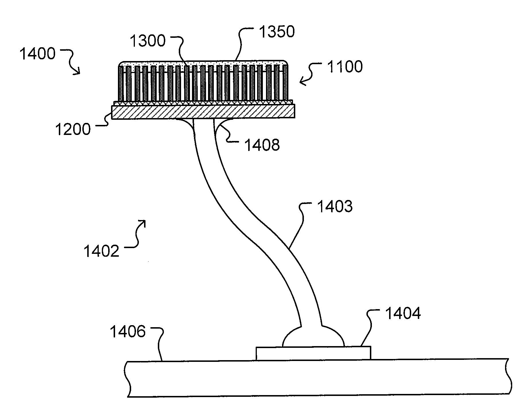
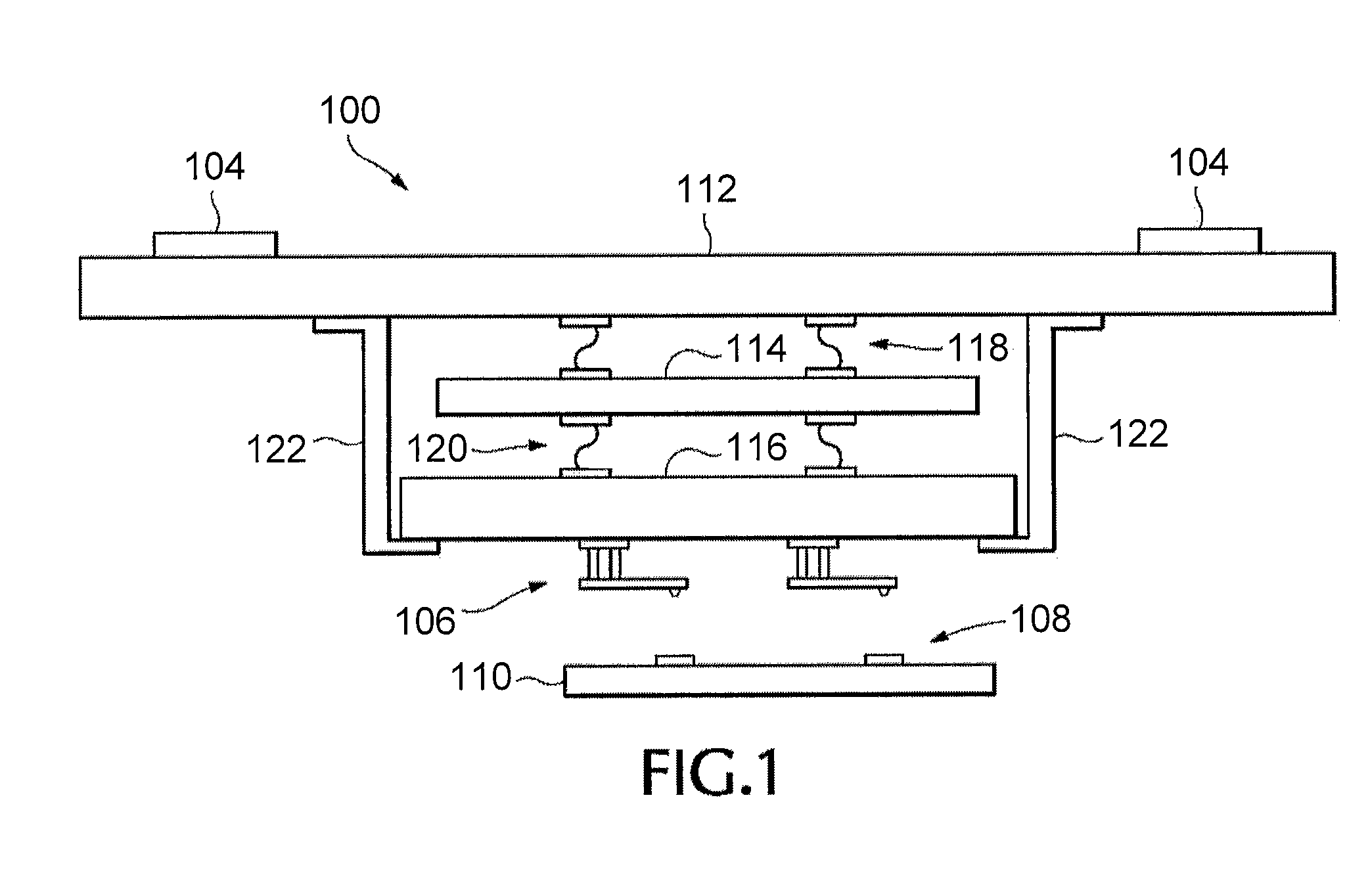
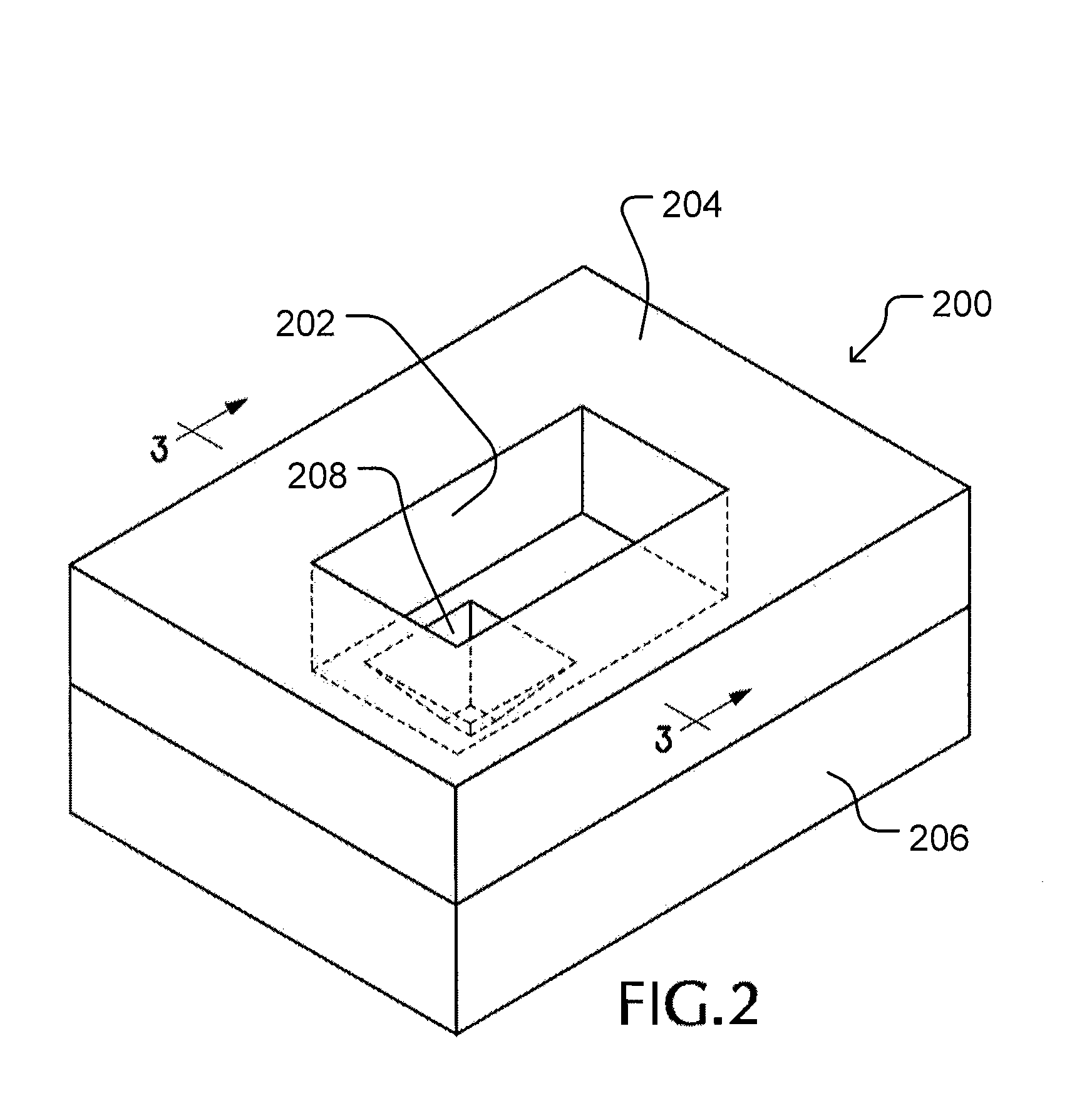
[0020]Exemplary embodiments of the invention now will be described more fully with reference to the accompanying drawings. This invention may, however, be embodied in many different forms and should not be construed as being limited to the embodiments and aspects set forth herein. Although the exemplary embodiments are described with respect to probe tips for testing semiconductor dies, the invention is not so limited but can be used in any probing application.
[0021]In general, some embodiments of the invention provide contact elements for a probe, which is also referred to herein as a contact structure. The contact elements, or the entire probe, may be made from carbon nanotube structures that have carbon nanotubes incorporated therein in a variety of ways. In one aspect, the carbon nanotubes may be grown on a film in a trench in which components of the probe are lithographically formed. In another aspect the carbon nanotubes may be in a plating solution that is used to plate a pro...
PUM
| Property | Measurement | Unit |
|---|---|---|
| thicknesses | aaaaa | aaaaa |
| length | aaaaa | aaaaa |
| width | aaaaa | aaaaa |
Abstract
Description
Claims
Application Information
 - R&D Engineer
- R&D Manager
- IP Professional
- Industry Leading Data Capabilities
- Powerful AI technology
- Patent DNA Extraction
Browse by: Latest US Patents, China's latest patents, Technical Efficacy Thesaurus, Application Domain, Technology Topic.
© 2024 PatSnap. All rights reserved.Legal|Privacy policy|Modern Slavery Act Transparency Statement|Sitemap