Light emitting element

a technology of light-emitting elements and organic compounds, which is applied in the direction of discharge tube luminescnet screens, organic semiconductor devices, natural mineral layered products, etc., can solve the problems of limited material mainly containing organic compounds which can transport electrons at a predetermined mobility or more, and achieve the effects of reducing the drive voltage, reducing the stress of the light-emitting layer, and suppressing the increase in the drive voltage over tim

Active Publication Date: 2010-06-15
SEMICON ENERGY LAB CO LTD
View PDF56 Cites 54 Cited by
  • Summary
  • Abstract
  • Description
  • Claims
  • Application Information

AI Technical Summary

Benefits of technology

[0009]Further, it is an object of the present invention to provide a display device in which the drive voltage is low and increase in the drive voltage over time is small and which can withstand long-term use.
[0010]Further, it is also an object of the present invention to improve the reliability of a light emitting element.
[0011]According to the present invention, a layer in contact with either of electrodes (a first electrode, a second electrode) in a light-emitting element is a hole-generating layer such as a layer containing a P-type semiconductor or an organic compound layer containing a material having electron-accepting properties, a light-emitting layer is provided between the hole-generating layers, and an electron-generating layer is formed between the hole-generating layer on the second electrode side and the light-emitting layer. This makes it possible to suppress the drive voltage. Further, increase in the drive voltage over time can be suppressed due to the lower drive voltage.
[0020]Further, a display device in which the drive voltage and increase in the drive voltage over time is small and which can withstand long-term use can be provided.
[0021]Still further, the stress in the light emitting layer can be alleviated. Accordingly, the reliability of the light emitting element can be improved.

Problems solved by technology

However, a material mainly containing an organic compound, to which electrons can be injected relatively easily from an electrode, or a material mainly containing an organic compound which can transport electrons at a predetermined mobility or more is very limited.

Method used


Image

  • Light emitting element
  • Light emitting element
  • Light emitting element

Examples


embodiment mode 1

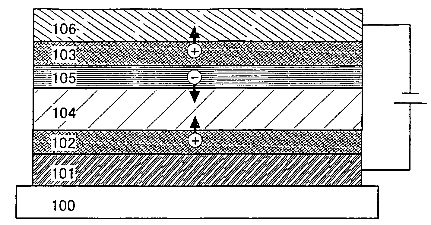
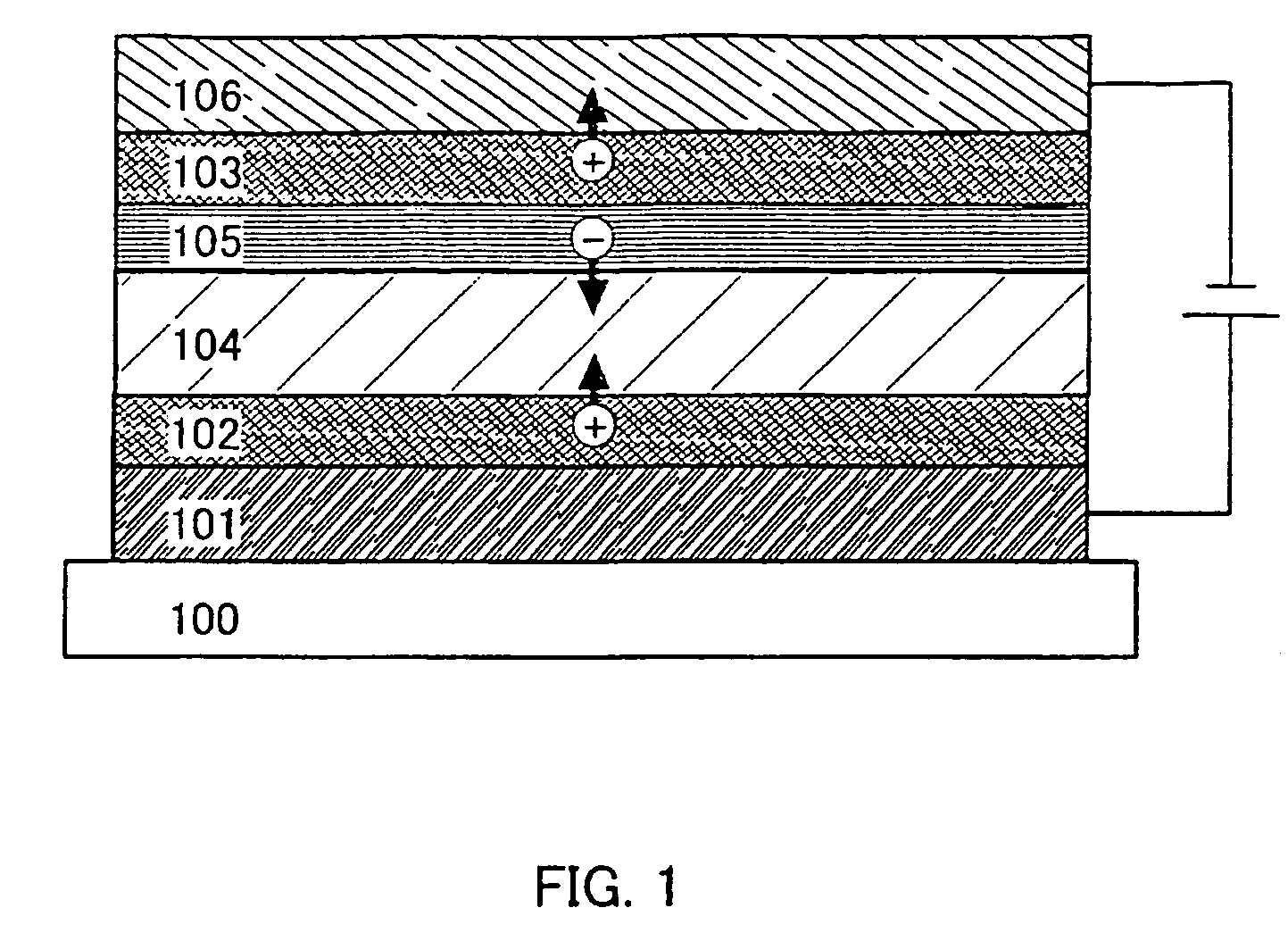
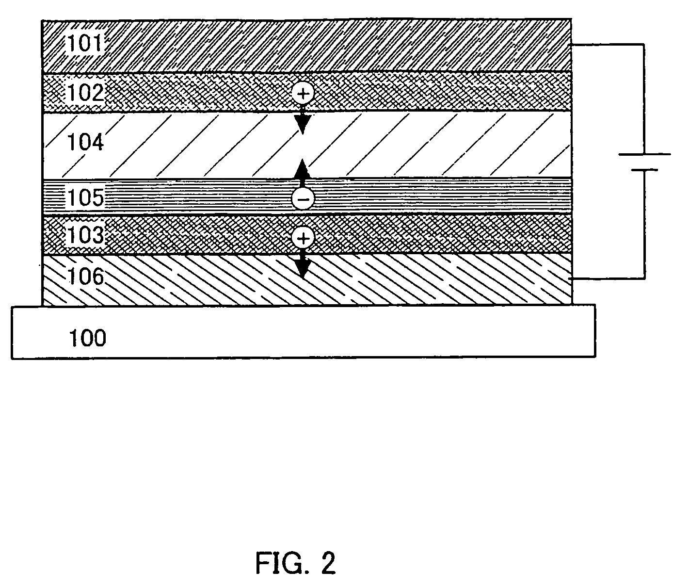
[0042]In the present embodiment mode, structures of a light-emitting element of the present invention will be described with reference to FIGS. 1 and 2. In a light-emitting element according to the present invention, a light-emitting layer 104 containing a light-emitting material and an electron-generating layer 105 are stacked, and the light-emitting layer 104 and the electron-generating layer 105 are provided between a first hole-generating layer 102 and a second hole-generating layer 103. The first hole generating layer 102 is in contact with a first electrode, and the second hole generating layer 103 is in contact with a second electrode. The first hole-generating layer 102 and the second hole-generating layer 103 are further provided between the first electrode 101 and the second electrode 106, and stacked over an insulator 100 such as a substrate or an insulating film. Over the insulator 100 such as the substrate or the insulating film, the first electrode 101, the first hole-...

embodiment mode 2

[0057]Another embodiment mode of the present invention will be described. The present embodiment mode describes an example of improving the characteristic of a viewing angle of a light-emitting element and a display device by appropriately adjusting the thicknesses of the first hole-generating layer 102 and the second hole-generating layer 103. Since the layered structure and the material of the light-emitting element in the present embodiment mode are the same as those in Embodiment Mode 1, the description is omitted here. Refer to Embodiment Mode 1. Note that, also in the present embodiment mode, when voltage is applied so as to make a light emitting element emit light, the electrode applied with higher potential is the first electrode, and the electrode applied with lower potential is the second electrode.

[0058]Light emitted from the light-emitting element includes light directly emitted from the light-emitting layer 104 and light emitted after being reflected once or multiple ti...

embodiment mode 3

[0074]This embodiment mode will describe a display device according to the present invention shown in Embodiment Mode 1 or Embodiment Mode 2 while showing its manufacturing method with reference to FIGS. 5A to 6C. Although this embodiment mode shows an example of manufacturing an active matrix display device, a light-emitting element of the present invention is also applicable for a passive matrix display device.

[0075]First, a first base insulating layer 51a and a second base insulating layer 51b are formed over a substrate 50, and then a semiconductor layer is formed over the second base insulating layer 51b (FIG. 5A).

[0076]As a material of the substrate 50, glass, quartz, plastic (such as polyimide, acrylic, polyethylene terephthalate, polycarbonate, polyacrylate, or polyethersulfone), or the like can be used. These substrates may be used after being polished by CMP or the like as necessary. In this embodiment mode, a glass substrate is used.

[0077]The first base insulating layer 5...


PUM


Abstract

It is an object of the present invention to provide a light-emitting element having a structure in which the drive voltage is relatively low. Further, it is an object of the invention to provide a highly reliable light emitting device by alleviating the stress to the light emitting layer. Further, it is another object of the invention to provide a light emitting element having a structure in which increase in the drive voltage over time is small. It is an object of the present invention to provide a display device in which the drive voltage is low and increase in the drive voltage over time is small and which can withstand long-term use. In a light emitting element, a layer in contact with an electrode serves as a hole generating layer such as an organic compound layer containing a P-type semiconductor or an electron accepting material, a light emitting layer is provided between hole generating layers, an electron generating layer is formed between the hole generation layer on the cathode side and the light emitting layer.

Description

TECHNICAL FIELD[0001]The present invention relates to a light-emitting element in which a thin film containing a light-emitting material is interposed between electrodes and which emits light when current is applied. Moreover, the present invention relates to a display device and an electronic appliance which use the light-emitting element.BACKGROUND ART[0002]A display using a thin film light-emitting element of a self-light-emitting type, which emits light by itself when current is applied, has been extensively developed.[0003]Such a thin film light-emitting element emits light by connecting an electrode to a single-layer or multilayer thin film formed using one or both of an organic compound and an inorganic compound when current is applied. Such a thin film light-emitting element is expected to reduce the power consumption, occupy smaller space, and increase the visibility, and the market is also expected to expand further.[0004]It has become possible to manufacture an element wh...

Claims


Application Information

Patent Timeline
Patent Type & Authority Patents(United States)
IPC IPC(8): H01J1/62
CPCH01L51/5052H01L51/506H01L51/5221H01L51/5068H01L27/3244H01L2251/5323H01L51/5265H01L2251/5315H10K59/12H10K50/155H10K50/157H10K50/165H10K50/828H10K50/852H10K2102/3031H10K2102/3026H05B33/20H05B33/26H05B33/10
Inventor KUMAKI, DAISUKESEO, SATOSHIYAMAZAKI, SHUNPEI
Owner SEMICON ENERGY LAB CO LTD
Why Eureka
Try Eureka