CMOS compatible integrated dielectric optical waveguide coupler and fabrication

a dielectric optical waveguide and integrated dielectric technology, applied in the direction of optical waveguide light guide, optical elements, instruments, etc., can solve the problems of low coupling loss, increase the complexity of device fabrication, and often suffer loss of coupling from optical fiber to photonic device with input and output waveguide, etc., to achieve efficient manufacturing and not affected by performance

Active Publication Date: 2010-06-15
GLOBALFOUNDRIES U S INC
View PDF26 Cites 38 Cited by
  • Summary
  • Abstract
  • Description
  • Claims
  • Application Information

AI Technical Summary

Benefits of technology

[0005]One embodiment of the present invention provides a method and structure for utilizing various dielectric materials in the formation of efficient optical couplers from optical fiber to optical devices within a semiconductor device. One embodiment of the present invention further provides a method for encapsulation of the devices and the formation of the couplers in a manner that is benign to the optical devices so that their performance is not affected. One embodiment of the invention also provides a CMOS compatible method that opens up ways for thermal treatment, electrical activation, and three-dimensional integration of optical devices. One embodiment of the present invention allows an efficiently manufactured semiconductor device that integrates photonics devices with CMOS circuit devices.

Problems solved by technology

Coupling from an optical fiber to a photonic device with input and output waveguides often suffers from loss due to index and mode-profile mismatches.
Polymer couplers have been demonstrated to provide effective matching and to result in low coupling losses.
Fabricating polymer couplers for use in applications wherein the photonic devices need to be encapsulated and annealed, as in many CMOS-compatible processes, presents fabrication difficulties that increases the complexity of device fabrication.

Method used


Image

  • CMOS compatible integrated dielectric optical waveguide coupler and fabrication
  • CMOS compatible integrated dielectric optical waveguide coupler and fabrication
  • CMOS compatible integrated dielectric optical waveguide coupler and fabrication

Examples


Embodiment Construction

[0022]While the specification concludes with claims defining the features of the invention that are regarded as novel, it is believed that the invention will be better understood from a consideration of the following description in conjunction with the drawing figures, in which like reference numerals are carried forward.

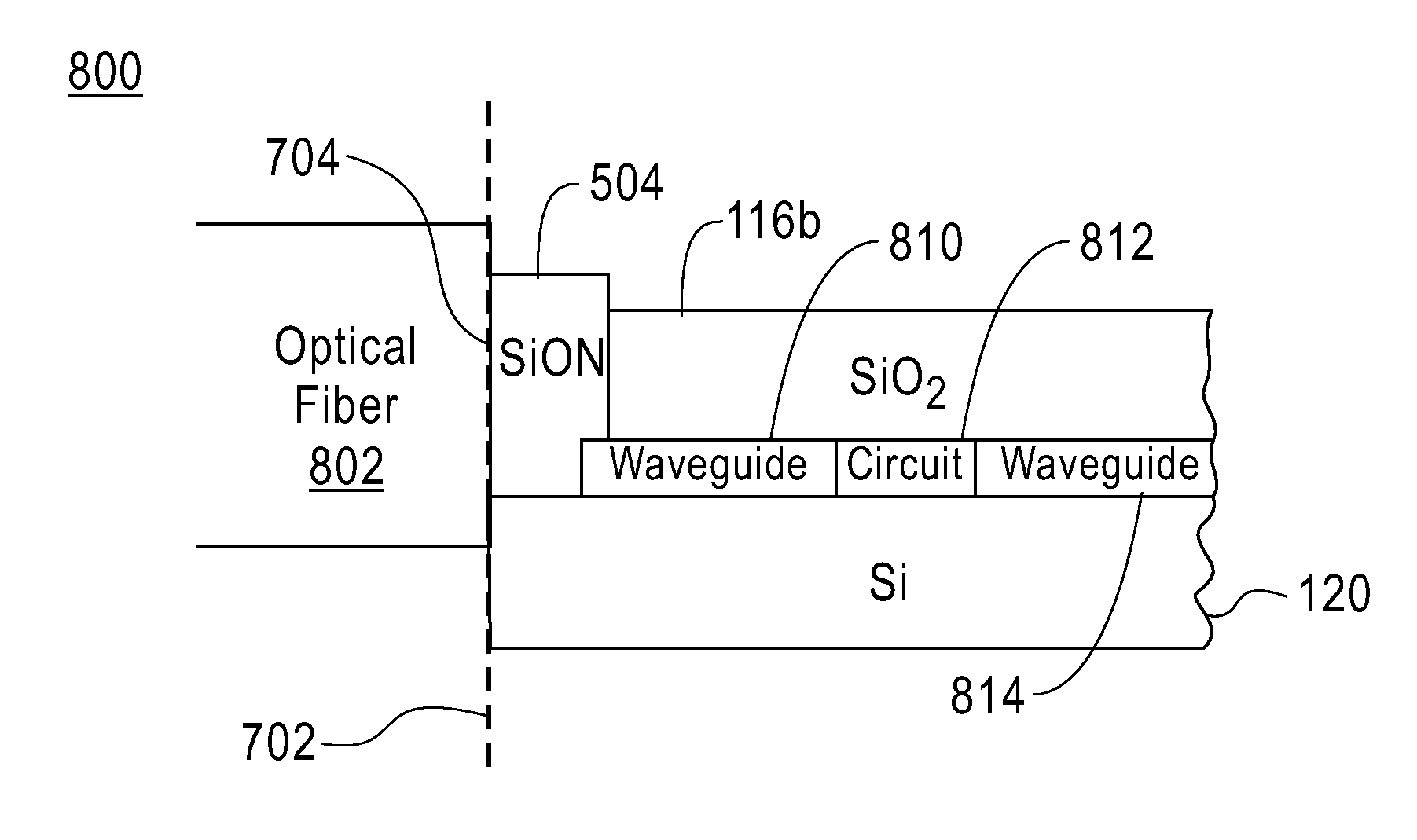
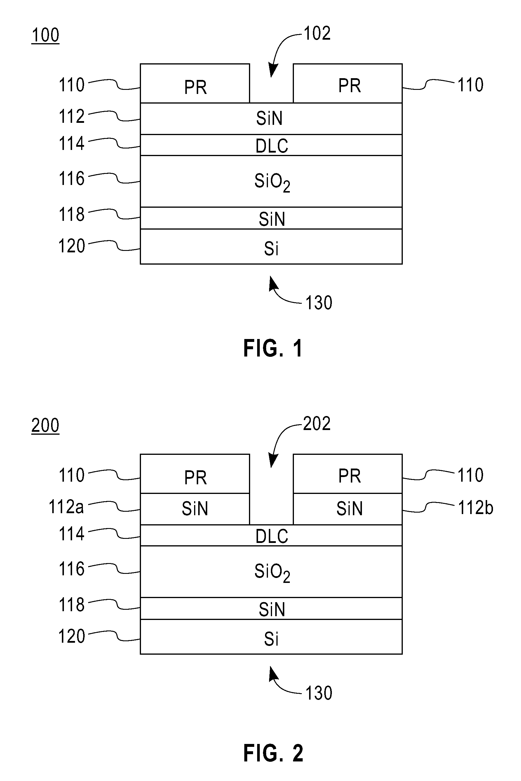
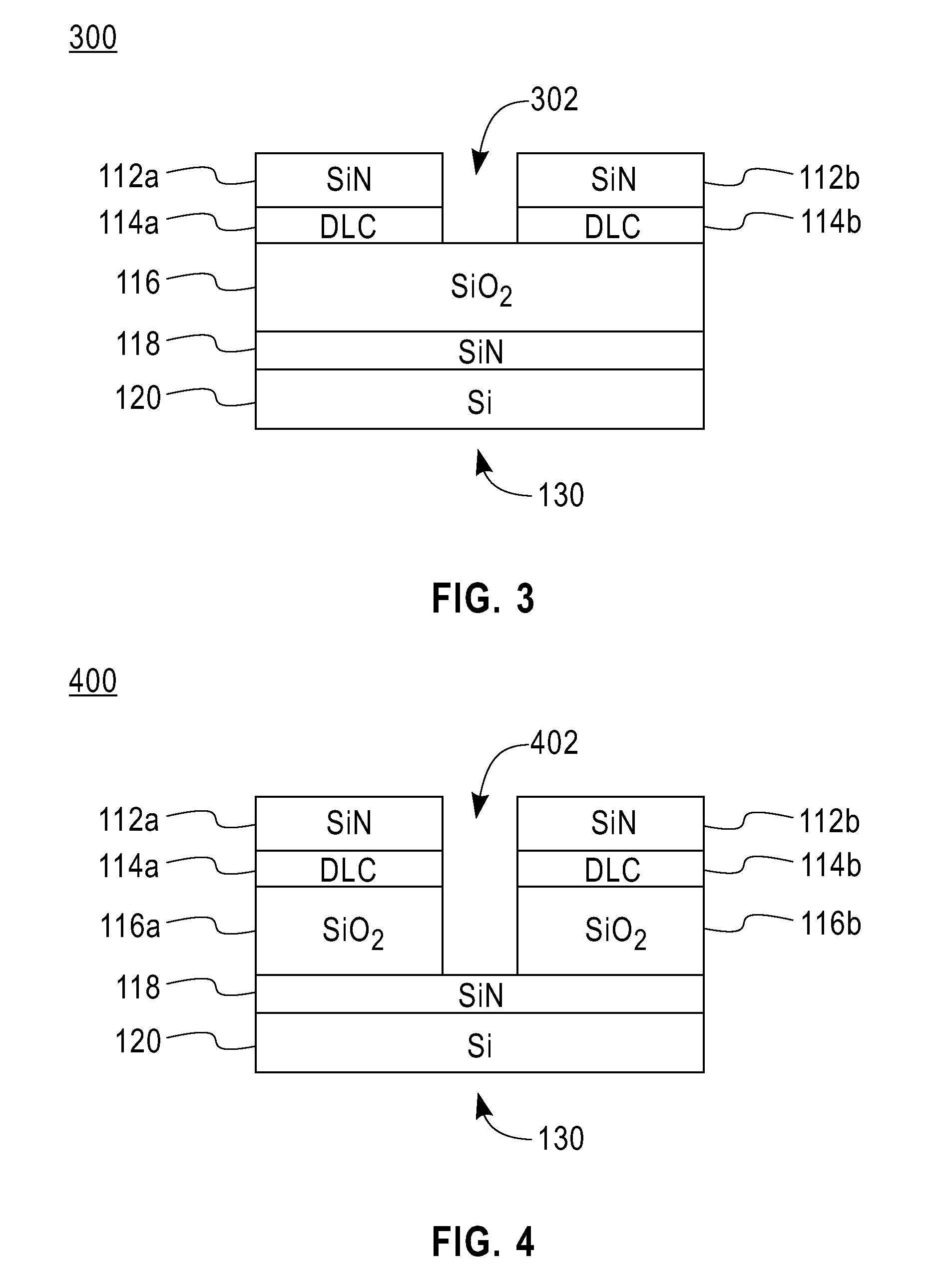
[0023]FIG. 1 illustrates a first fabrication phase 100 for a silicon based semiconductor die 130, in accordance with one embodiment of the present invention. The first fabrication phase 100 shows a silicon based semiconductor die 130 that has an integrated silicon device 120 consisting of conventional integrated electronic and / or optoelectronic circuits fabricated on a single semiconductor substrate. In one embodiment, the silicon based semiconductor die 130 includes electronic circuits and / or optoelectronic circuits that include, for example, embedded silicon optical waveguide structures that have been fabricated on the silicon device 120 according to conventional ...


PUM

PropertyMeasurementUnit
refractive indexaaaaaaaaaa
dielectric optical transitionaaaaaaaaaa
optical coupling transitionaaaaaaaaaa

Abstract

An optoelectronic circuit fabrication method and integrated circuit apparatus fabricated therewith. Integrated circuits are fabricated with an integral optical coupling transition to efficiently couple optical energy from an optical fiber to an integrated optical waveguide on the integrated circuit. Layers of specific materials are deposited onto a semiconductor circuit to support etching of a trench to receive an optical coupler that performs proper impedance matching between an optical fiber and an on-circuit optical waveguide that extends part way into the transition channel. A silicon based dielectric that includes at least a portion with a refractive index substantially equal to a section of the optical fiber is deposited into the etched trench to create the optical coupler. Silicon based dielectrics with graded indices are also able to be used. Chemical mechanical polishing is used finalize preparation of the optical transition and integrated circuit.

Description

FIELD OF THE INVENTION[0001]The present invention relates generally to silicon circuit devices and fabrication techniques, and more particularly to forming integrated optical waveguide couplers onto optoelectronic circuits.BACKGROUND OF THE INVENTION[0002]Integrated semiconductor devices that include one or more photonic devices, such as photodetectors, modulators, optical switches, and the like, require a mechanism to couple optical signals between the optical fibers used to communicate optical signals to and from the semiconductor device and the silicon based waveguides that are within the semiconductor devices and used to deliver the optical signals to the photonic devices within the integrated semiconductor devices. Coupling from an optical fiber to a photonic device with input and output waveguides often suffers from loss due to index and mode-profile mismatches.[0003]Polymer couplers are one technique used to minimize losses in coupling between an optical fiber and input and o...

Claims


Application Information

Patent Timeline
Patent Type & Authority Patents(United States)
IPC IPC(8): G02B6/12G02B6/10H01L21/302
CPCB82Y20/00G02B6/30G02B6/1223
Inventor ASSEFA, SOLOMONJAHNES, CHRISTOPHERVLASOV, YURII
Owner GLOBALFOUNDRIES U S INC
Why Eureka
Try Eureka