Method of fabricating an embedded circuit pattern

a technology of embedded circuits and patterns, applied in the field of substrates, can solve the problems of inherently slow process and high associated cost, and achieve the effect of quick method and low cos

Active Publication Date: 2010-07-13
AMKOR TECH SINGAPORE HLDG PTE LTD
View PDF176 Cites 33 Cited by
  • Summary
  • Abstract
  • Description
  • Claims
  • Application Information

AI Technical Summary

Benefits of technology

[0010]In one embodiment, the embedded circuit pattern has an absence of dimples. Accordingly, a dimple free embedded circuit pattern is formed without use of over-plate and / or over-etch processes. By avoiding over-plate and / or over-etch processes, the embedded circuit pattern is fabricated using a relatively quick method and thus at a low cost.

Problems solved by technology

Although the over-plate process and over-etch process are effective in producing a circuit pattern, the processes are inherently slow and thus have a high associated cost.

Method used


Image

  • Method of fabricating an embedded circuit pattern
  • Method of fabricating an embedded circuit pattern
  • Method of fabricating an embedded circuit pattern

Examples


Embodiment Construction

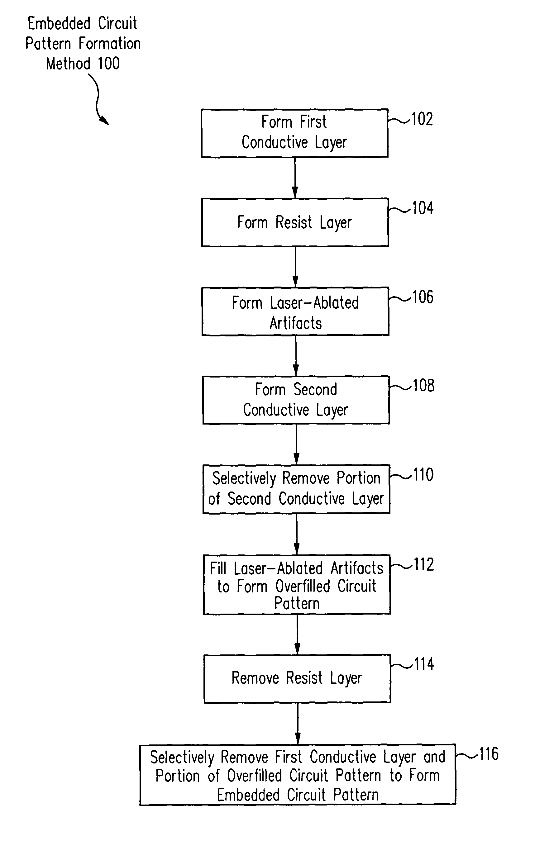
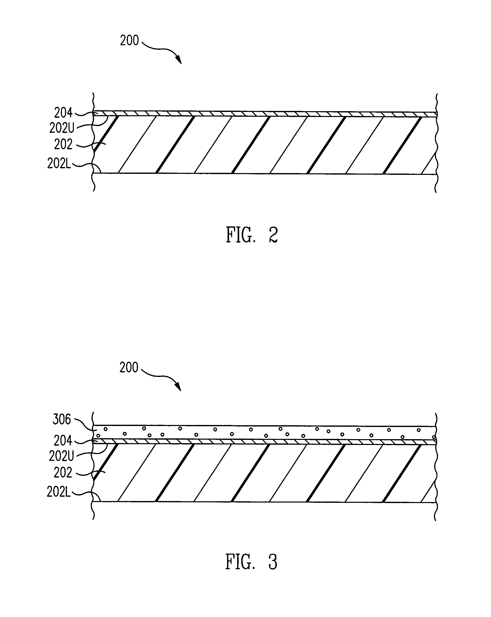
[0019]In accordance with one embodiment, referring to FIGS. 4 and 5 together, a method of fabricating a substrate 200 includes forming a first conductive layer 204 on a dielectric layer 202, forming a resist layer 306 on first conductive layer 204, and forming laser-ablated artifacts 408 through first resist layer 306, through first conductive layer 204, and at least partially into dielectric layer 202.

[0020]Referring to FIG. 6, a second conductive layer 626 is formed on resist layer 306 and within laser-ablated artifacts 408. Referring to FIG. 7, a portion of second conductive layer 626 is selectively removing such that second conductive layer 626 remains only within laser-ablated artifacts 408. Referring to FIG. 8, laser-ablated artifacts 408 are filled to form an overfilled circuit pattern 830.

[0021]Referring to FIGS. 8 and 9 together, resist layer 306 is removed. Referring to FIGS. 9 and 10 together, first conductive layer 204 is removed and a portion of overfilled circuit patte...


PUM

PropertyMeasurementUnit
conductiveaaaaaaaaaa
electrically conductiveaaaaaaaaaa
heightaaaaaaaaaa

Abstract

A method of fabricating a substrate includes forming a first conductive layer on a dielectric layer, forming a resist layer on the first conductive layer, and forming laser-ablated artifacts through the first resist layer, through the first conductive layer, and at least partially into the dielectric layer. A second conductive layer is formed within the laser-ablated artifacts. The laser-ablated artifacts are filled to form an overfilled circuit pattern. The resist layer and the first conductive layer are removed. Further, a portion of the overfilled circuit pattern is removed to form an embedded circuit pattern embedded within the dielectric layer.

Description

BACKGROUND OF THE INVENTION[0001]1. Field of the Invention[0002]The present invention relates generally to substrates for mounting of electronic components. More particularly, the present invention relates to a method of fabricating an embedded circuit pattern and the resulting structure.[0003]2. Description of the Related Art[0004]To form a circuit pattern, features in a dielectric layer are filled with plated copper. To prevent the formation of dimples in the plated copper as well as to ensure that the features are completely filled, an over-plate process is typically used.[0005]During this over-plate process, the features are overfilled with plated copper such that the copper not only fills the features but also is plated with a significant thickness across the entire substrate.[0006]The over-plate process is followed by an over-etch process. During this over-etch process, the excess plated copper is removed by etching. Further, to ensure that all of the excess plated copper is r...

Claims


Application Information

Patent Timeline
Patent Type & Authority Patents(United States)
IPC IPC(8): H01K3/10
CPCH05K3/045H05K3/107H05K3/0038H05K3/027Y10T29/49167H05K2203/0723Y10T29/49165
Inventor RUSLI, SUKIANTOHUEMOELLER, RONALD PATRICK
Owner AMKOR TECH SINGAPORE HLDG PTE LTD
Why Eureka
Try Eureka