Image display apparatus and projection optical system
a technology of optical system and display apparatus, which is applied in the field of image forming apparatuses, can solve the problems of deteriorating the yield rate of liquid crystal panels, increasing costs, and reducing the open area ratio
- Summary
- Abstract
- Description
- Claims
- Application Information
AI Technical Summary
Benefits of technology
Problems solved by technology
Method used
Image

Examples
first embodiment
[0061]A description will now be given, with reference to FIGS. 4A and 4B, of an image display apparatus according to the present invention. It should be noted that parts that are the same as the parts shown in FIGS. 1 through 3 are given the same reference numerals.
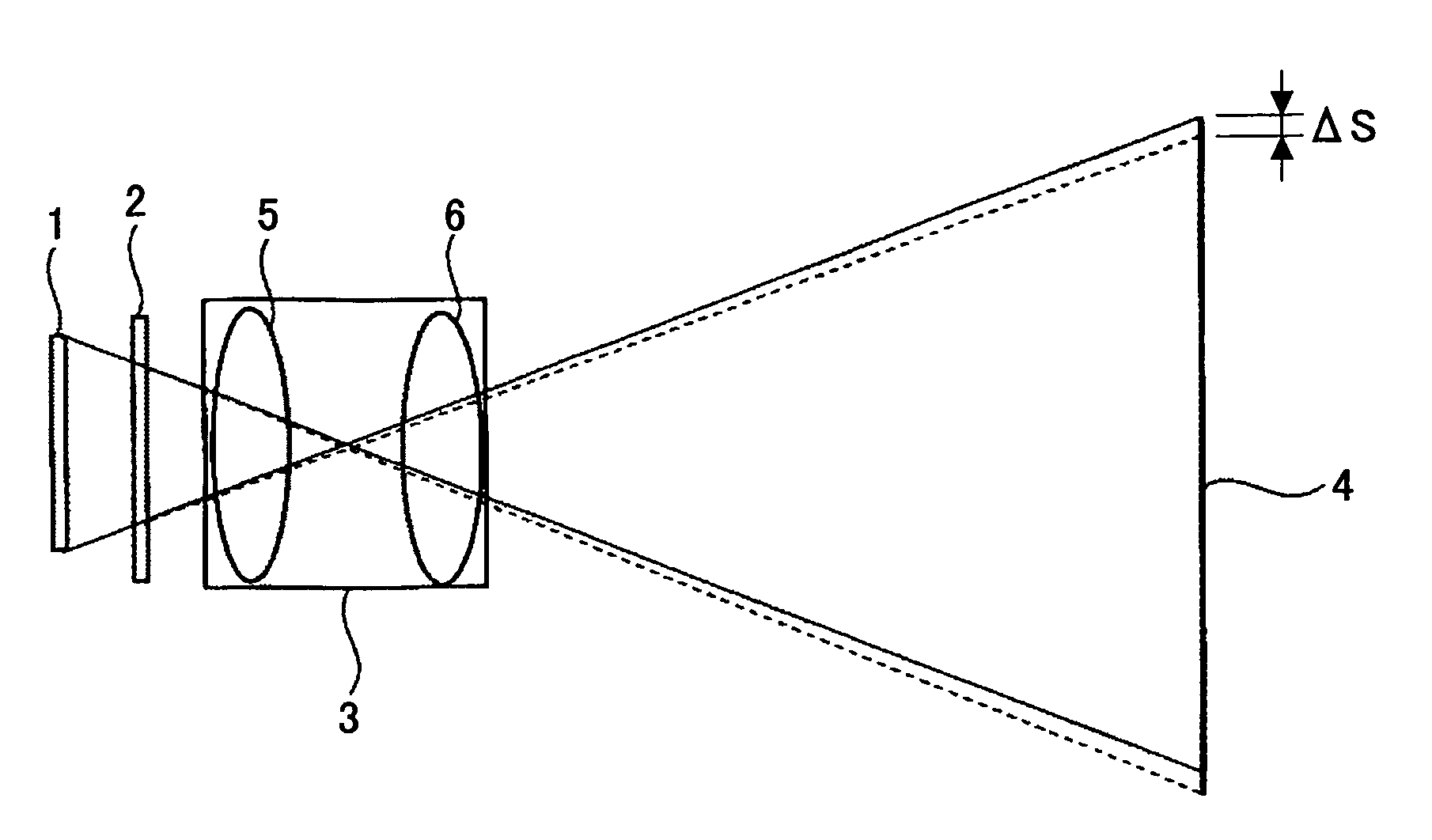
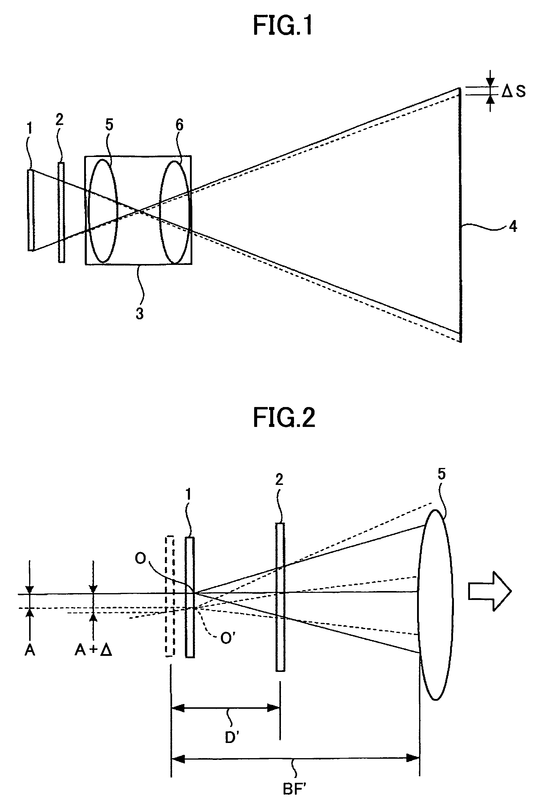
[0062]As shown in FIG. 4A, the image display apparatus 10 according to the first embodiment of the present invention comprises: a light source for illumination (not shown in the figure); a light valve 1 as a spatial light modulation element that displays an image; an optical path deflecting element 2 that deflects an optical path in accordance with a signal of the image formed on the light valve 1; and an objection optical system 3. The optical path deflecting element 2 is provided within the projection optical system 3.
[0063]The projection optical system 3 projects a light, which is modulated by a spatial light modulation element such as a liquid crystal device, a reflection type dot matrix liquid crystal device, a digit...
fourth embodiment
[0084]A description will now be given, with reference to FIG. 9, of an image display apparatus according to the present invention. In the present embodiment, a display area can be enlarged, and the picture elements displayed on the light valve 1 are effectively used so that an aspect ratio can be changed without deteriorating resolution. In order to achieve the above-mentioned feature, an amount of shift of a picture element by the optical path deflecting element 2 is set to be equal to a plurality of picture elements so as to apparently change a display size.
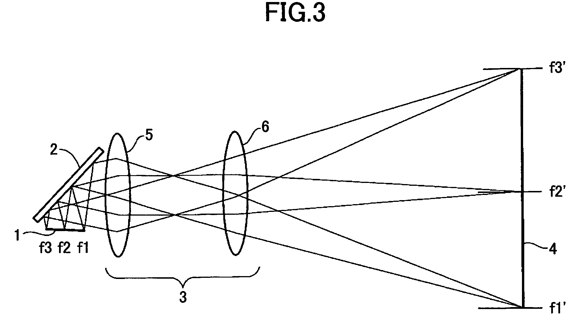
[0085]FIG. 9 shows a screen (1), which has no picture element shift, and a screen (2), which is picture-element-shifted. Both the screens are overlapped with each other by an amount of shift ΔS indicated by (3). In the figure, each small square □ corresponds to a picture element. It should be noted that one side of the square □ in the figure is about a half of one side of the spatial light modulation element since the light mod...
fifth embodiment
[0087]A description will now be given, with reference to FIG. 10, of the present invention. In the present embodiment, a display area is enlarged and an apparent resolution in a center portion is increased so as to achieve an image display of a higher quality.
[0088]A density of picture elements in an overlapping area (6) in FIG. 10 can be doubled by further performing a ½ picture element shift on the overlapping area (5) shown in FIG. 9 in the above-mentioned fourth embodiment. This technique enables an increase in resolution in a center portion, especially, in television or the like.
PUM
| Property | Measurement | Unit |
|---|---|---|
| aspect ratio | aaaaa | aaaaa |
| optical path | aaaaa | aaaaa |
| distance | aaaaa | aaaaa |
Abstract
Description
Claims
Application Information