Reducing silicon attack and improving resistivity of tungsten nitride film
What is AI technical title?
AI technical title is built by Patsnap AI team. It summarizes the technical point description of the patent document.
a technology of tungsten nitride and resistivity, which is applied in the direction of semiconductor devices, electrical equipment, semiconductor/solid-state device details, etc., can solve the problems of forming defects and the same difficulties of deposition of other tungsten-containing layers on silicon, and achieve the effect of reducing the attack of tungsten precursors
Active Publication Date: 2010-07-13
NOVELLUS SYSTEMS
View PDF69 Cites 51 Cited by
Summary
Abstract
Description
Claims
Application Information
AI Technical Summary
This helps you quickly interpret patents by identifying the three key elements:
Problems solved by technology
Method used
Benefits of technology
Problems solved by technology
One difficulty in replacing Ti / TiN with WN on silicon is that the WF6 precursor commonly used to deposit WN may attack the silicon, forming defects.
Deposition of other tungsten-containing layers on silicon presents the same difficulties.
Method used
Image
Click on the blue label to locate the original text in one second.
Reading with bidirectional positioning of images and text.
Examples
Embodiment Construction
[0017]Introduction
[0018]As indicated, the present invention provides methods for depositing tungsten-containing layers, especially for applications in which the tungsten-containing layer is deposited over silicon surfaces and wherein thin, conformal and adhesive layers are required. The present invention also provides methods of depositing tungsten-containing films over Ti / TiN films and other substrates.
[0019]Deposition of tungsten-containing films by methods such as pulsed nucleation layer (PNL), atomic layer deposition (ALD) and chemical vapor deposition (CVD) on silicon involves use of a tungsten precursor, often WF6. At the conditions typically used for deposition, the substrate surface may be susceptible to attack by the tungsten precursor. For example, deposition of a tungsten nitride film by PNL involves reacting a tungsten precursor with an adsorbed layer of a reducing agent. Typical PNL deposition temperatures are around 300 C. At this temperature and other PNL processing c...
PUM
Property
Measurement
Unit
temperature
aaaaa
aaaaa
thickness
aaaaa
aaaaa
thick
aaaaa
aaaaa
Abstract
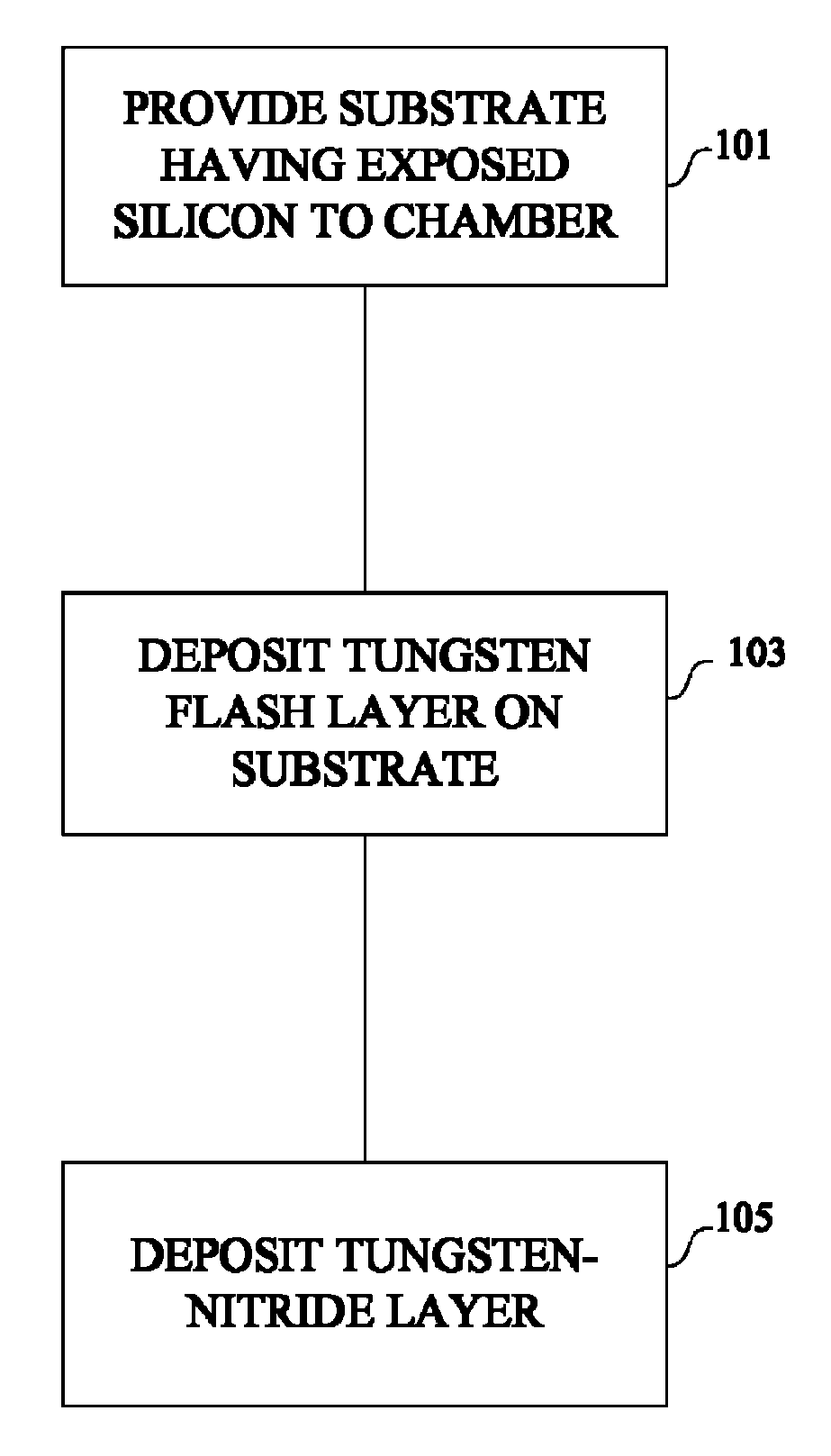
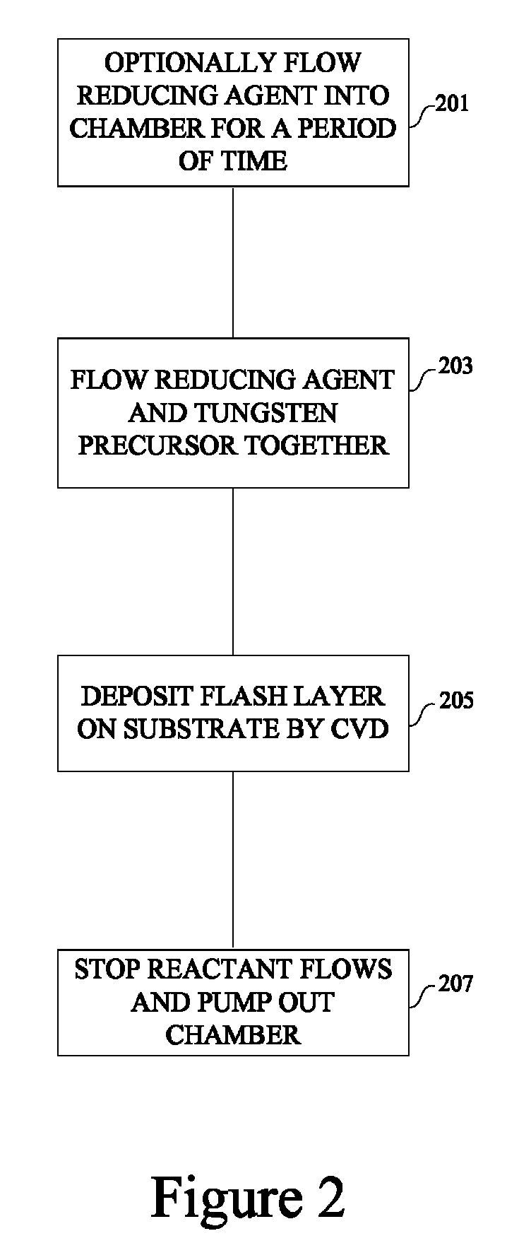
The present invention provides improved methods of depositing tungsten-containing films on substrates, particularly on silicon substrates. The methods involve depositing an interfacial or “flash” layer of tungsten on the silicon prior to deposition of tungsten nitride. The tungsten flash layer is typically deposited by a CVD reaction of a tungsten precursor and a reducing agent. According to various embodiments, the tungsten flash layer may be deposited with a high reducing agent to tungsten-precursor ratio and / or at low temperature to reduce attack by the tungsten precursor. In many cases, the substrate is a semiconductor wafer or a partially fabricated semiconductor wafer. Applications include depositing tungsten nitride as (or as part of) a diffusion barrier and / or adhesion layer for tungsten contacts.
Description
CROSS-REFERENCE TO RELATED PATENT APPLICATIONS[0001]This application is a continuation-in-part of U.S. application Ser. No. 10 / 649,351, now issued as U.S. Pat. No. 7,141,494, filed Aug. 26, 2003, entitled METHOD FOR REDUCING TUNGSTEN FILM ROUGHNESS AND IMPROVING STEP COVERAGE which is incorporated herein by reference in its entirety. This application is related to the following: U.S. application Ser. No. 09 / 975,074 (issued as U.S. Pat. No. 6,635,965) filed Oct. 9, 2001, entitled ULTRA THIN TUNGSTEN LAYER WITH IMPROVED STEP COVERAGE, U.S. patent application Ser. No. 10 / 690,492, (issued as U.S. Pat. No. 7,005,372) filed Oct. 20, 2003, entitled DEPOSITION OF TUNGSTEN NITRIDE FILM, U.S. patent application Ser. No. 10 / 815,560, (issued as U.S. Pat. No. 7,262,125) filed Mar. 31, 2004, entitled METHOD OF FORMING LOW-RESISTIVITY TUNGSTEN INTERCONNECTS and U.S. patent application Ser. No. 11 / 265,531, filed Nov. 1, 2005, entitled METHOD FOR GROWING LOW RESISTIVITY TUNGSTEN FILM.FIELD OF THE IN...
Claims
Application Information
Patent Timeline
Application Date:The date an application was filed.
Publication Date:The date a patent or application was officially published.
First Publication Date:The earliest publication date of a patent with the same application number.
Issue Date:Publication date of the patent grant document.
PCT Entry Date:The Entry date of PCT National Phase.
Estimated Expiry Date:The statutory expiry date of a patent right according to the Patent Law, and it is the longest term of protection that the patent right can achieve without the termination of the patent right due to other reasons(Term extension factor has been taken into account ).
Invalid Date:Actual expiry date is based on effective date or publication date of legal transaction data of invalid patent.

