Method of forming a contact structure including a vertical barrier structure and two barrier layers

a contact structure and vertical barrier technology, applied in the direction of resistors, basic electric elements, solid-state devices, etc., can solve the problems of unpredictable circuit operation, unpredictable memory cell operation, unpredictable memory cell operation, etc., to prevent the electrical properties of the integrated circuit device from being affected, improve the reliability of the circui

Inactive Publication Date: 2006-07-04
MICRON TECH INC
View PDF26 Cites 32 Cited by
  • Summary
  • Abstract
  • Description
  • Claims
  • Application Information

AI Technical Summary

Benefits of technology

[0007]The above mentioned problems with coupling devices in integrated circuits and other problems are addressed by the present invention and will be understood by reading and studying the following specification. A contact structure is described that includes one or more layers and other structures for blocking atomic migration in an integrated circuit, which improves the reliability of the circuit.
[0008]The present invention provides, in one embodiment, a contact including a polysilicon layer formed on a substrate, one or more barrier layers formed above the polysilicon layer, and a barrier structure encircling the polysilicon layer and the one or more barrier layers. The polysilicon layer provides a conductive material for coupling to an active or a passive device in an integrated circuit. At least one of the one or more barrier layers restricts the migration of atoms to and from the substrate, and at least one of the one or more barrier layers restricts the migration of oxygen atoms. Restricting the migration of substrate atoms, prevents the electrical properties of the integrated circuit devices from being inadvertently altered during circuit fabrication. Restricting the migration of oxygen atoms, deters oxidation at electrode surfaces, such as capacitor electrode surfaces. Since the barrier layers of the contact are also electrically conductive, the contact is suitable for use in interconnecting integrated circuit devices.
[0009]In an alternate embodiment, the present invention provides a method of fabricating a contact. The method includes forming a polysilicon layer and a tungsten nitride layer above a base integrated circuit structure. The polysilicon layer is formed at an electrical connection site of an integrated circuit device. The polysilicon layer and the tungsten nitride layer are etched to a level below the surface of the base integrated circuit structure. The polysilicon layer encircling the contact is etched much deeper, and a silicon nitride layer is formed to encircle the tungsten nitride layer. A ruthenium silicide layer is formed above the tungsten nitride layer as an oxygen barrier. The silicon nitride layer prevents the polysilicon layer from reacting with the ruthenium silicide layer. After polishing and cleaning, the ruthenium silicide layer is ready for coupling to an integrated circuit device.

Problems solved by technology

Unfortunately, several problems arise when a non-silicon electrode is directly coupled to a MOSFET drain or source.
First, the electrode can experience oxidation, which interferes with the electrode conductivity and may cause unpredictable memory cell operation.
Atomic migration alters the electrical properties of the integrated circuit elements and may cause unpredictable memory cell operation.
Unfortunately, a single barrier layer that effectively blocks both oxygen migration and atomic migration from the substrate may react with the conductive layer fabricated at the source or drain and cause unpredictable circuit operation.

Method used


Image

  • Method of forming a contact structure including a vertical barrier structure and two barrier layers
  • Method of forming a contact structure including a vertical barrier structure and two barrier layers
  • Method of forming a contact structure including a vertical barrier structure and two barrier layers

Examples


Embodiment Construction

[0023]In the following detailed description of the preferred embodiments, reference is made to the accompanying drawings which form a part hereof, and in which is shown by way of illustration specific preferred embodiments in which the invention may be practiced. These embodiments are described in sufficient detail to enable those skilled in the art to practice the invention, and it is to be understood that other embodiments may be utilized and that logical, mechanical and electrical changes may be made without departing from the spirit and scope of the present inventions. The following detailed description is, therefore, not to be taken in a limiting sense, and the scope of the present invention is defined only by the appended claims.

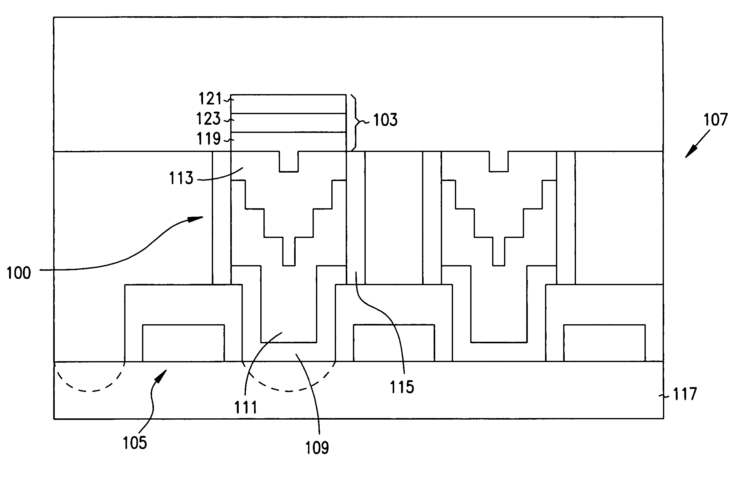
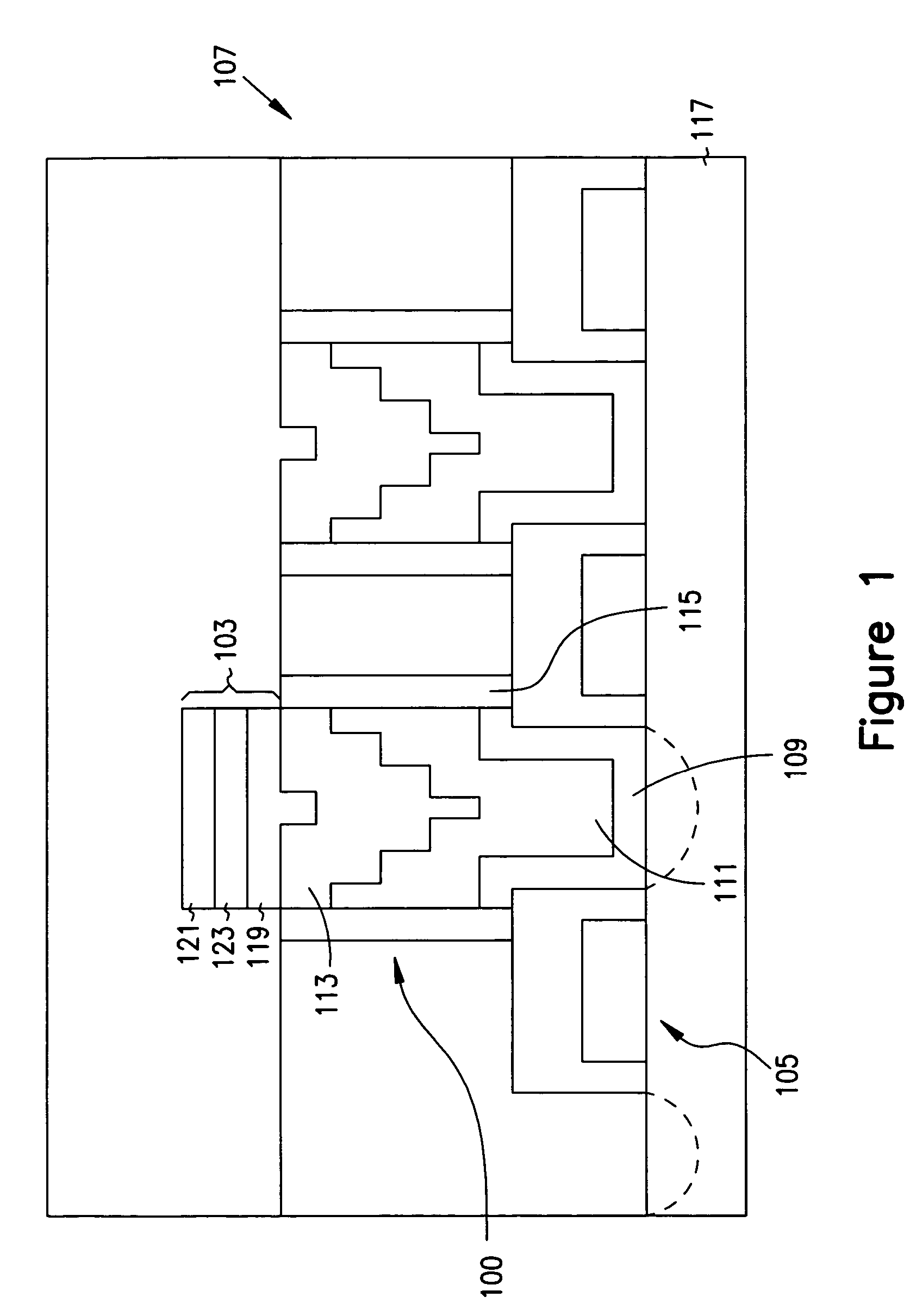
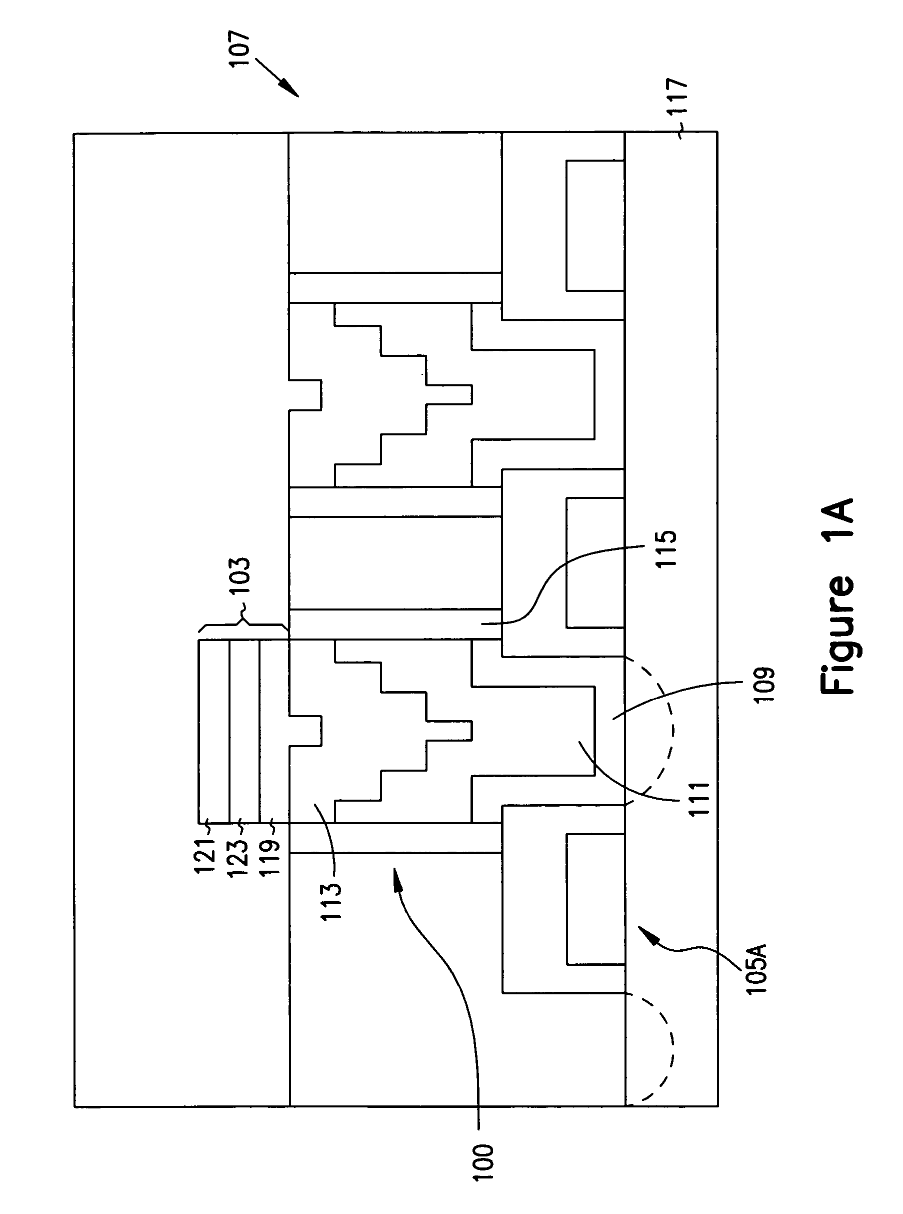
[0024]FIG. 1 is an illustration of one embodiment of contact structure 100 coupling device 103 to device 105 in integrated circuit 107. Contact structure 100 provides a conductive path for transmitting an electrical signal between devices 103 and 105. ...


PUM

PropertyMeasurementUnit
thicknessaaaaaaaaaa
thicknessaaaaaaaaaa
thicknessaaaaaaaaaa

Abstract

This invention relates to contact structures for use in integrated circuits and methods of fabricating contact structures. In one embodiment, a contact structure includes a conductive layer, one or more barrier layers formed above the conductive layer, and a barrier structure encircling the polysilicon layer and the one or more barrier layers. In an alternate embodiment, a contact structure is fabricated by forming a polysilicon layer on a substrate, forming a tungsten nitride layer above the polysilicon layer, and etching the polysilicon layer and the tungsten nitride layer to a level below the surface of a substrate structure. A silicon nitride layer is formed above the tungsten nitride layer, and a ruthenium silicide layer is formed above the silicon nitride layer. The ruthenium silicide layer is then polished.

Description

[0001]This application is a Divisional of U.S. application Ser. No. 09 / 653,640, filed Aug. 31, 2000 now U.S. Pat. No. 6,787,833, which is incorporated herein by reference.FIELD OF THE INVENTION[0002]This invention relates to contact structures, and more particularly to contact structures used in the fabrication of integrated circuits.BACKGROUND OF THE INVENTION[0003]An integrated circuit, such as a dynamic random access memory (DRAM) includes passive devices, such as capacitors, and active devices, such as metal-oxide semiconductor field-effect transistors (MOSFETS), fabricated on a single substrate. In fabricating an integrated circuit to perform a particular function, the passive and active devices are coupled together. For example, a capacitor electrode is electrically coupled to a MOSFET drain or source to form a dynamic random access memory (DRAM) cell for storing information.[0004]One method of coupling a capacitor electrode to a MOSFET drain or source includes the operation o...

Claims


Application Information

Patent Timeline
Patent Type & Authority Patents(United States)
IPC IPC(8): H01L21/8242H01L21/20H01L21/44H01L21/4763H01L21/768H01L21/8234H01L23/48H01L27/108H01L29/74H01L29/76H01L31/119
CPCH01L21/76802H01L21/76831H01L21/7687H01L21/76877H01L27/10855H01L2924/0002H01L2924/00H10B12/0335
Inventor FISHBURN, FRED
Owner MICRON TECH INC
Why Eureka
Try Eureka