Printed circuit board having embedded electronic component and method of manufacturing the same

Inactive Publication Date: 2012-06-28
SAMSUNG ELECTRO MECHANICS CO LTD
View PDF3 Cites 8 Cited by
  • Summary
  • Abstract
  • Description
  • Claims
  • Application Information

AI Technical Summary

Benefits of technology

[0009]Accordingly, the present invention has been made keeping in mind the problems encountered in the related art and the present invention is intended to provide a PCB having an embedded electronic component and a method of manufacturing the same, in which metal bumps formed on an electroni

Problems solved by technology

However, conventional embedded PCBs and manufacturing methods thereof are disadvantageous because vias are used to form electrical connections with electronic components (elements), which undesirably increases the processing cost and complicates the manufacturing process, and also because low peel strength between the insulating layer and the plating layer upon forming the plating layer on the insulating layer may weaken the force of adhesio

Method used


Image

  • Printed circuit board having embedded electronic component and method of manufacturing the same
  • Printed circuit board having embedded electronic component and method of manufacturing the same
  • Printed circuit board having embedded electronic component and method of manufacturing the same

Examples


second embodiment

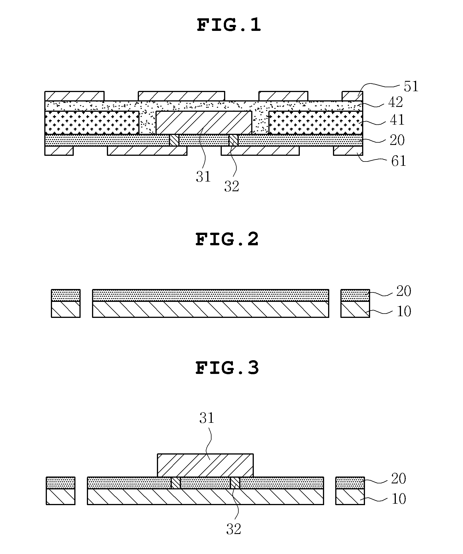
[0050]In order to protect the roughness for supplementing the supporting force of the polymer layer 20 and ensuring the peel strength upon plating of a metal layer, a carrier member may be formed on the polymer layer 20. Specifically, upon preparing the polymer layer, the polymer layer may be provided in the form of the carrier member having been attached thereto, and the carrier member may be removed after forming the second insulating layer on one side of the first insulating layer having the opening. Below, the PCB manufacturing process including attaching the carrier member 10 to the polymer layer 20 is described.

first embodiment

[0051]Below, the description that overlaps with the description of the method of manufacturing the PCB having an embedded electronic component is omitted.

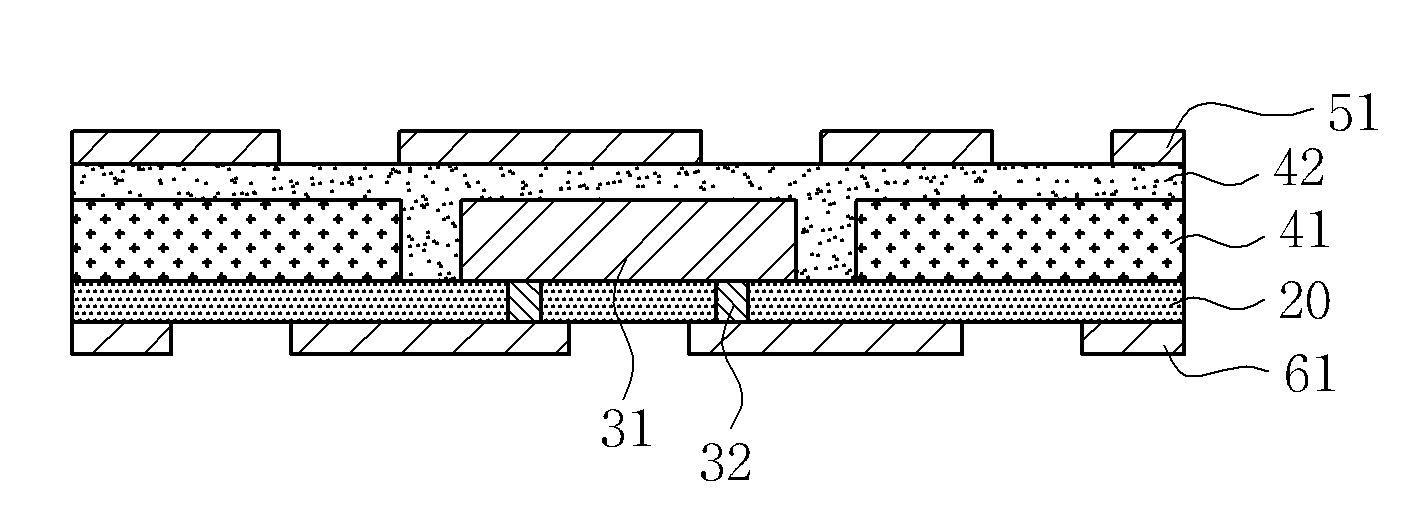
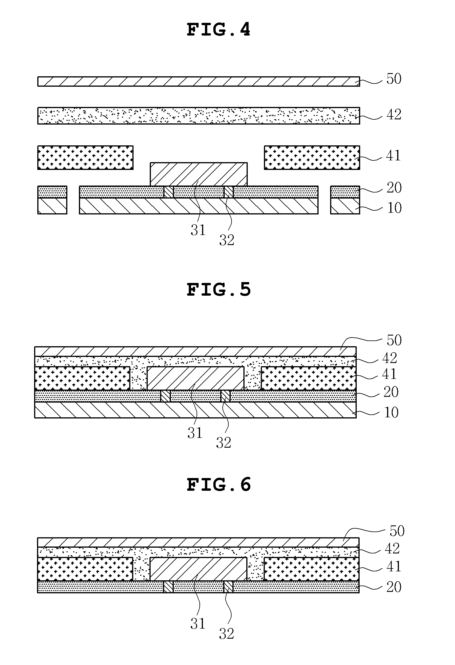
[0052]FIG. 9 shows forming the polymer layer 20 on the carrier member 10, and FIG. 10 shows forming the first insulating layer 41 having the opening for mounting the electronic component 31. The electronic component 31 may be directly seated on the polymer layer 20 thus manufacturing a PCB having an embedded electronic component. The PCB manufacturing process may be conducted using the carrier member 10 for supplementing the supporting force of the polymer layer 20. As such, the carrier member 10 is separated and removed during the subsequent PCB manufacturing process. Whereas the electronic component 31 is seated on the polymer layer 20 and then the first insulating layer 41 having the opening is formed thereon so that the electronic component 31 is disposed in the opening in the first embodiment, the first insulating layer 41 ha...


PUM

PropertyMeasurementUnit
Thicknessaaaaaaaaaa
Surface roughnessaaaaaaaaaa
aaaaaaaaaa

Abstract

Disclosed is a printed circuit board having an embedded electronic component, which includes a first insulating layer, an electronic component disposed in an opening formed in a thickness direction of the first insulating layer and having a metal bump, a polymer layer formed on one side of the first insulating layer and on which the electronic component is seated so that the metal bump of the electronic component perforates the polymer layer, a second insulating layer formed on the other side of the first insulating layer so as to embed the electronic component, a first circuit layer formed on the second insulating layer, and a second circuit layer formed on the polymer layer so as to be directly electrically connected to the metal bump that perforates the polymer layer, and in which roughness is formed on the polymer layer so that the force of adhesion of the polymer layer to a plating layer is enhanced, thus ensuring reliability of the electrical connection of a circuit layer which is subsequently formed.

Description

CROSS REFERENCE TO RELATED APPLICATION[0001]This application claims the benefit of Korean Patent Application No. 10-2010-0132715, filed Dec. 22, 2010, entitled “A printed circuit board comprising embedded electronic component within and a method for manufacturing,” which is hereby incorporated by reference in its entirety into this application.BACKGROUND OF THE INVENTION[0002]1. Technical Field[0003]The present invention relates to a printed circuit board (PCB) having an embedded electronic component and a method of manufacturing the same.[0004]2. Description of the Related Art[0005]Typically circuit boards include a variety of active and passive elements such as resistors, capacitors, inductors, transformers, filters, mechanical switches, relays and so on. On the other hand, electronic devices are configured such that respective elements are systematically connected so that they can efficiently perform their original functions. Thus, when power is applied to circuits, various passi...

Claims


Application Information

Patent Timeline
IPC IPC(8): H05K1/09H05K1/16H05K1/02H05K3/30
CPCH01L23/5389H05K1/185H05K2201/0355H05K2201/10674H05K2203/0152Y10T29/4913H05K2203/1152H05K2203/1189H05K2203/1469H01L24/19H05K2203/063H01L2224/04105
Inventor JEONG, TAE SUNGLEE, DOO HWANLEE, SEUNG EUN
Owner SAMSUNG ELECTRO MECHANICS CO LTD
Why Eureka
Try Eureka