Methods for forming contact hole, for manufacturing circuit board and for manufacturing electro-optical device

a technology of contact hole and manufacturing method, which is applied in the direction of optics, programmable/customizable/modifiable circuits, instruments, etc., can solve the problems of high manufacturing cost, conductive material cannot reach the surface of the first electrode, and wire breaking is likely to occur on the projections, so as to prevent the breakage of the wire coupling between the first electrode and the second electrode, improve the reliability of the manufacturing electro-optical device itself, and improve the reliability of the second

Inactive Publication Date: 2006-02-02
SEIKO EPSON CORP
View PDF3 Cites 21 Cited by
  • Summary
  • Abstract
  • Description
  • Claims
  • Application Information

AI Technical Summary

Benefits of technology

[0010] According to one aspect, the present invention provides a method for forming a contact hole, a method for manufacturing a circuit board and a method for manufacturing an electro-optical device that increase the reliability of electrical coupling and prevent wire-breaking due to projections when forming a contact hole in an interlayer film by using a needle, and burying a conductive material in the contact hole.
[0021] According to this aspect, since the method for forming a circuit board is used, breakage of the wire coupling the first electrode to the second electrode is prevented while the reliability of electrical coupling is improved. Thus, the reliability of the manufactured electro-optical device itself can be improved.

Problems solved by technology

However, using photolithography and etching involves pattern-forming, which complicates the manufacturing steps and requires vacuum equipment and many chemicals, resulting in higher manufacturing costs.
Therefore, in burying a conductive material in the contact holes, the conductive material can not reach the surface of the first electrode since the contact holes are blocked halfway.
If wires coupled to the contacts are formed on the interlayer film in this state, wire-breaking is likely to occur on the projections.

Method used


Image

  • Methods for forming contact hole, for manufacturing circuit board and for manufacturing electro-optical device
  • Methods for forming contact hole, for manufacturing circuit board and for manufacturing electro-optical device
  • Methods for forming contact hole, for manufacturing circuit board and for manufacturing electro-optical device

Examples


Embodiment Construction

[0028] Illustrative embodiments of the present invention will be described below in detail.

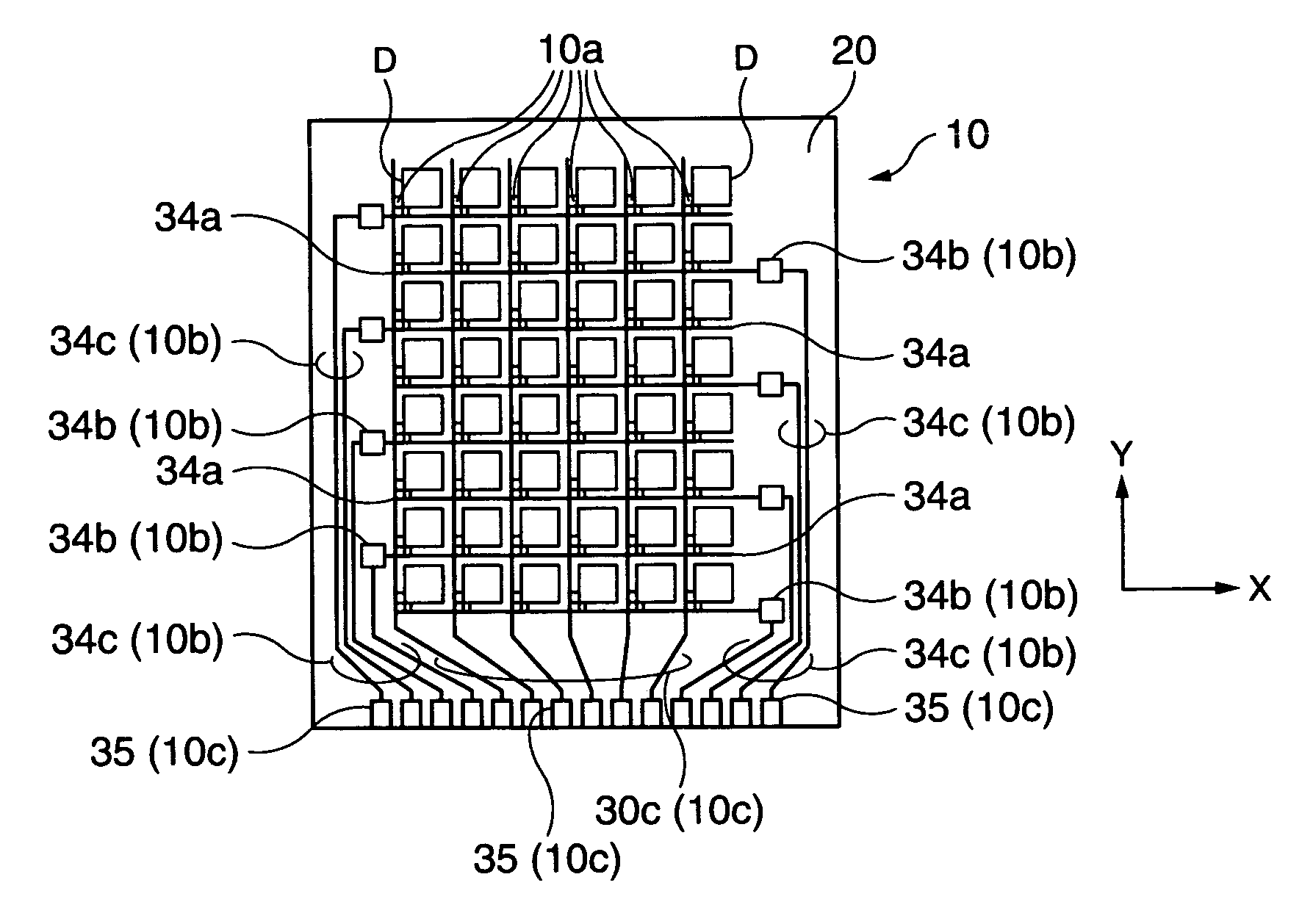
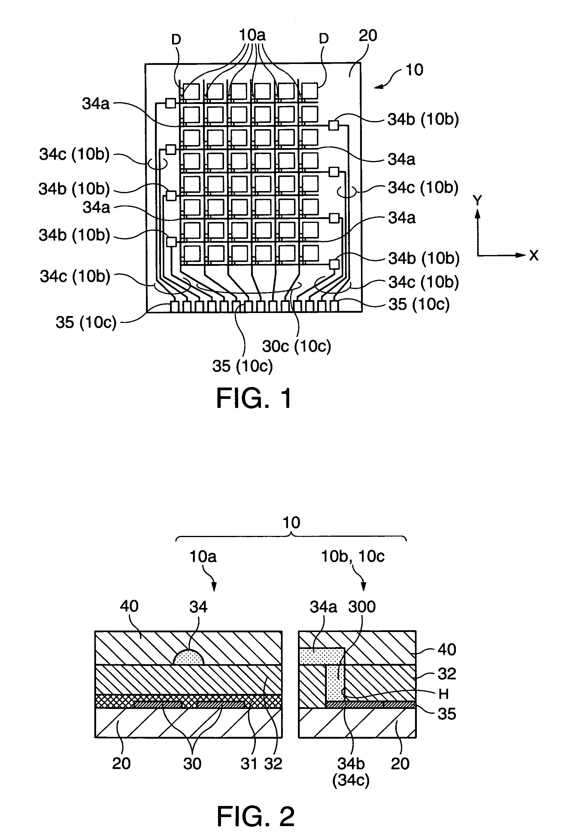
[0029]FIG. 1 is a diagram showing a circuit board manufactured by employing a method for forming a contact hole according to a first embodiment of the invention. A circuit board 10 is illustrated in FIG. 1.

[0030] Referring to FIG. 1, the circuit board 10 includes a plurality of organic thin-film transistors 10a, a plurality of gate lines 34a and a plurality of pixel electrodes D substantially centered on a rectangle substrate 20, for example. Gate line coupling parts 34b are formed on an outer circumference part 10b along the longitudinal side direction of the circuit board 10. External coupling terminals 35 coupled to gate lead wires 34c from the gate line coupling parts 34b or source lead wires 30c are formed on an outer circumference part 10c along one short side of the circuit board 10.

[0031]FIG. 2 is a side sectional view of the circuit board 10 along the X-direction in FIG. 1.
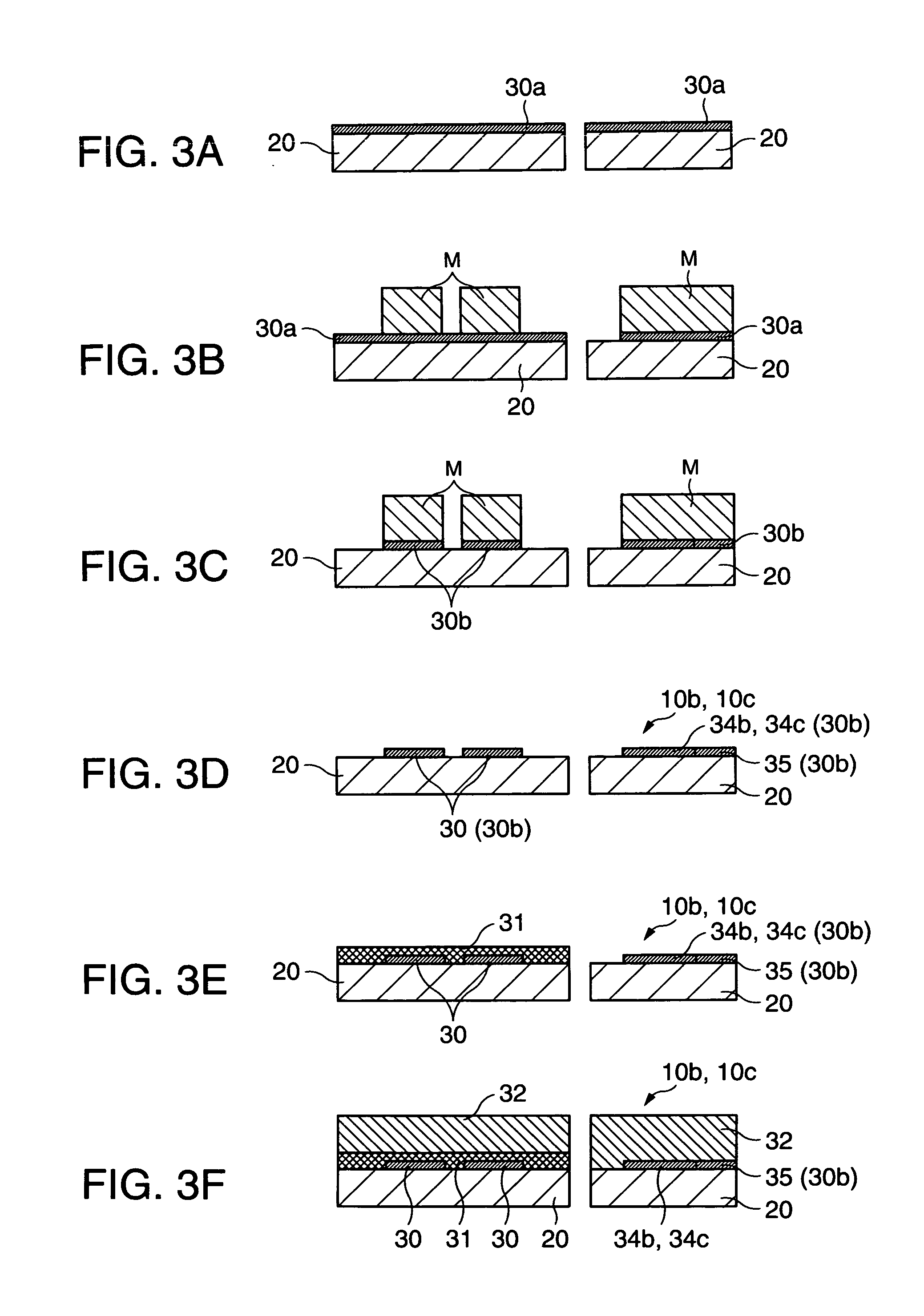
[0032] ...


PUM

PropertyMeasurementUnit
diameteraaaaaaaaaa
electrically conductiveaaaaaaaaaa
conductiveaaaaaaaaaa

Abstract

A method for forming a contact hole, a method for manufacturing a circuit board and a method for manufacturing an electro-optical device that increase the reliability of electrical coupling via a conductive part and prevent wire-breaking due to projections when forming a contact hole in an interlayer film by using a needle, and burying a conductive material in the contact hole is provided.

Description

RELATED APPLICATIONS [0001] This application claims priority to Japanese Application No. 2004-218872, filed Jul. 27, 2004, whose contents are explicitly incorporated herein by reference. FIELD OF THE INVENTION [0002] The present invention relates to a method for forming a contact hole, a method for manufacturing a circuit board and a method for manufacturing an electro-optical device such as a liquid crystal device, an organic electro-luminescence (EL) device and an electrophoretic device. BACKGROUND OF THE INVENTION [0003] For a semiconductor element, a technique has been known to establish electrical coupling between electrodes provided on different layers over a circuit board. According to the technique as described in Japanese Unexamined Patent Publication No. 10-96960 for example, contact holes are formed by using photolithography and etching, and then an electrically conductive material is buried in the contact holes for providing electrical coupling between the electrodes. [0...

Claims


Application Information

Patent Timeline
Patent Type & Authority Applications(United States)
IPC IPC(8): H01L21/4763G02F1/167
CPCG02F1/1345G02F1/167H01L2924/0002H01L21/76802H01L27/283H01L27/3274H01L27/3276H01L51/56H05K1/0289H05K3/002H05K3/005H05K2203/0126H05K2203/0221H05K2203/0783H01L2924/00H05K3/4069H10K19/10H10K59/125H10K59/131H10K71/00H01L21/28H01L21/3205
Inventor HARADA, MITSUAKIMORIYA, SOICHI
Owner SEIKO EPSON CORP
Why Eureka
Try Eureka