Semiconductor structure and process thereof

a technology of semiconductor structure and dielectric layer, which is applied in the direction of semiconductor devices, basic electric elements, electrical equipment, etc., can solve the problems of inferior performance, inferior thickness of gate dielectric layer, and conventional poly-silicon gate face, so as to improve the effective work function value of semiconductor structure and increase electrical reliability

Active Publication Date: 2013-05-09
UNITED MICROELECTRONICS CORP
View PDF10 Cites 22 Cited by
  • Summary
  • Abstract
  • Description
  • Claims
  • Application Information

AI Technical Summary

Benefits of technology

[0009]The present invention provides a semiconductor structure with a fluoride work function metal layer, and process thereof. Since the work function metal layer contains fluorine ions, the work function metal layer can have a work function value closer to that of the bandwidth. Thus, the effective work function value of the semiconductor structure is improved. Besides, the fluorine ions of the fluoride work function metal layer can diffuse into the dielectric layer below, so that the NBTI (negative bias temperature instability) value decreases, and the electrical reliability increases.

Problems solved by technology

With the trend towards scaling down the size of semiconductor devices, conventional poly-silicon gates face problems, such as inferior performance due to boron penetration and unavoidable depletion effect.
This increases the equivalent thickness of the gate dielectric layer, reduces the gate capacitance, and decreases the driving force of the devices.
As semiconductor technologies are miniaturized to the nanometer scale, work function metal gate structures are close to their physical and electrical limitations, giving rise to problems of electrical unreliability of the gate structures, such as degraded NBTI values (negative bias temperature instability).
For a complementary metal-oxide semiconductor (CMOS), dual work function metal gates need to be paired with an NMOS component and a PMOS component; integrated technologies and process controls of components are therefore more complicated, and the process efficiency restrained.

Method used


Image

  • Semiconductor structure and process thereof
  • Semiconductor structure and process thereof
  • Semiconductor structure and process thereof

Examples


Embodiment Construction

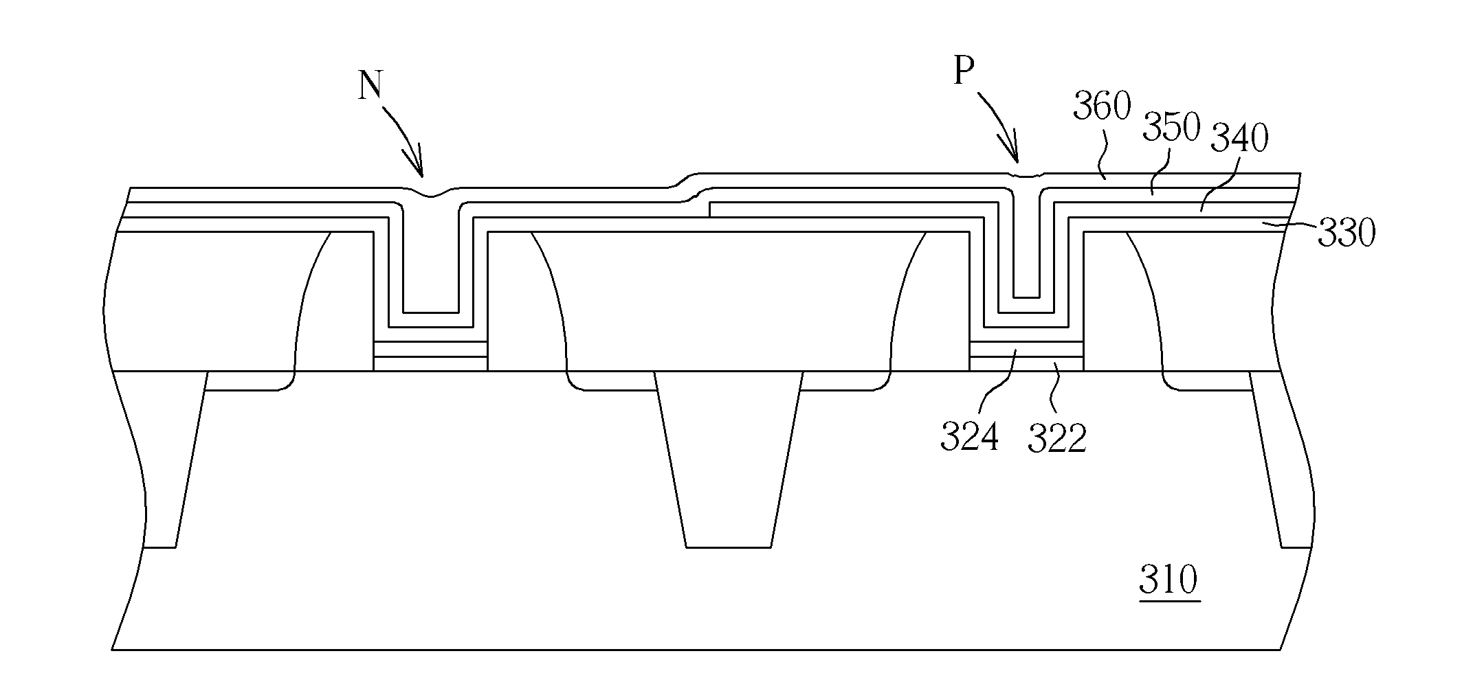
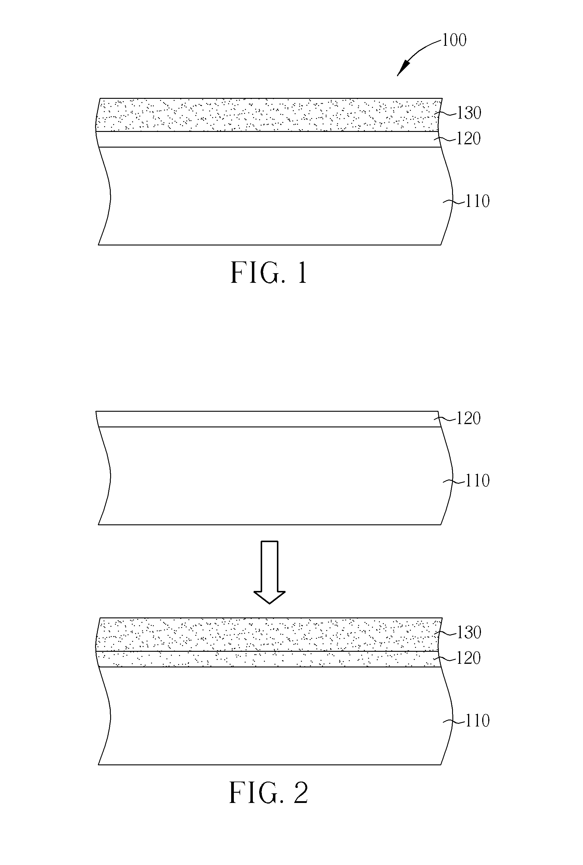
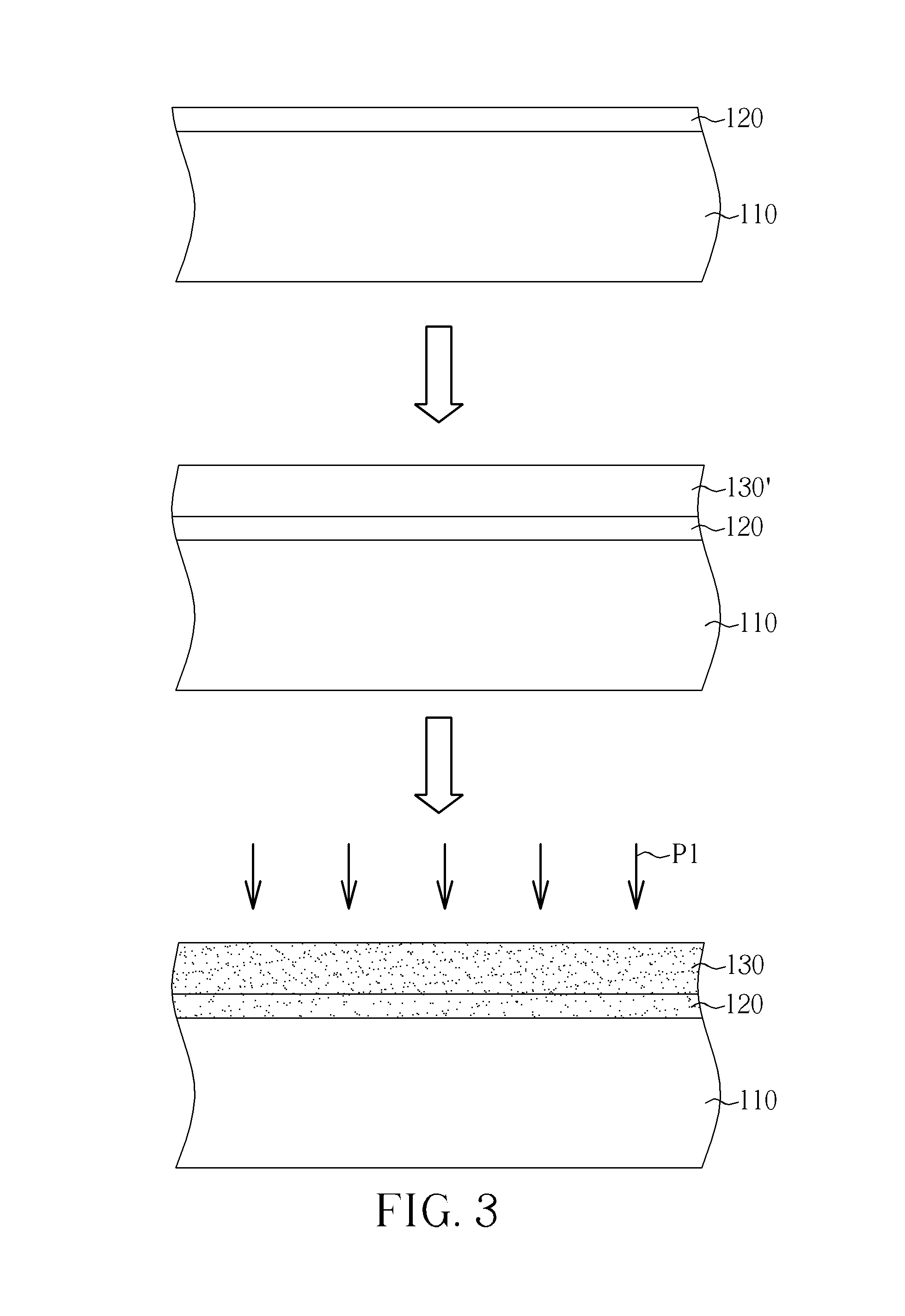
[0016]FIG. 1 schematically depicts a cross-sectional view of a semiconductor structure according to one embodiment of the present invention. As shown in FIG. 1, a semiconductor structure 100 includes a substrate 110, a dielectric layer 120 and a fluoride metal layer 130. The dielectric layer 120 is located on the substrate 110. The fluoride metal layer 130 is located on the dielectric layer 120. The substrate 110 may be a semiconductor substrate such as a silicon substrate, a silicon containing substrate, a III-V group-on-silicon (such as GaN-on-silicon) substrate, a graphene-on-silicon substrate or a silicon-on-insulator (SOI) substrate. The dielectric layer 120 may be a dielectric layer having a high dielectric constant, such as a metal containing dielectric layer, including hafnium oxide or zirconium oxide etc. The dielectric layer having a high dielectric constant maybe the group selected from hafnium oxide (HfO2), hafnium silicon oxide (HfSiO4), hafnium silicon oxynitride (HfSi...


PUM

PropertyMeasurementUnit
work functionaaaaaaaaaa
dielectric constantaaaaaaaaaa

Abstract

A semiconductor structure includes a substrate, a dielectric layer and a fluoride metal layer. The dielectric layer is located on the substrate. The fluoride metal layer is located on the dielectric layer. Furthermore, the present invention also provides a semiconductor process to form said semiconductor structure.

Description

BACKGROUND OF THE INVENTION[0001]1. Field of the Invention[0002]The present invention relates generally to a semiconductor structure and process thereof, and more specifically, to a semiconductor structure having a fluoride metal layer, and process thereof.[0003]2. Description of the Prior Art[0004]Poly-silicon is conventionally used as a gate electrode in semiconductor devices like metal-oxide-semiconductors (MOS). With the trend towards scaling down the size of semiconductor devices, conventional poly-silicon gates face problems, such as inferior performance due to boron penetration and unavoidable depletion effect. This increases the equivalent thickness of the gate dielectric layer, reduces the gate capacitance, and decreases the driving force of the devices. Therefore, work function metals that are suitable to serve as high-K gate dielectric layers are used to replace the conventional poly-silicon gate to be the control electrode.[0005]As semiconductor technologies are miniatur...

Claims


Application Information

Patent Timeline
Patent Type & Authority Applications(United States)
IPC IPC(8): H01L29/78H01L21/28
CPCH01L21/265H01L21/28088H01L29/4966H01L21/823842H01L29/517H01L29/66545H01L29/513
Inventor LIN, KUN-HSIENLIN, CHUN-HSIENHUANG, HSIN-FU
Owner UNITED MICROELECTRONICS CORP
Why Eureka
Try Eureka