Circuit board process

a technology of circuit board and process, applied in the field of circuit board process, can solve the problems of reducing the adverse effect of the reliability of the circuit board, and achieve the effect of increasing the circuit board fabrication efficiency

Inactive Publication Date: 2008-08-21
UNIMICRON TECH CORP
View PDF3 Cites 8 Cited by
  • Summary
  • Abstract
  • Description
  • Claims
  • Application Information

AI Technical Summary

Benefits of technology

[0009]Accordingly, the present invention is directed to a circuit board process for improving the fabrication efficiency on a circuit board.
[0010]According to another aspect of the present invention, a circuit board process is provided for improving the alignment accuracy on a circuit board.
[0011]According to yet another aspect of the present invention, a circuit board process is provided for improving the circuit reliability on a circuit board.
[0024]According to the present invention, the dispositions of a circuit layer and a conductive hole are defined in the same process. Compared to conventional techniques, less numbers of alignment process are required for defining the dispositions of the conductive hole and the circuit layer, therefore the circuit fabrication efficiency can be effectively increased. Moreover, since the dispositions of the circuit layer and the conductive hole are defined in the same process, the alignment accuracy regarding the relative positions between the conductive hole and the circuit may be unaffected by the process tolerance.

Problems solved by technology

Thus, the conventional technique requires several alignment processes for defining the dispositions of the conductive hole 160 and the second circuit layer 130′, which reduces circuit fabrication efficiency on the circuit board.
On the other hand, in a circuit board fabricated by the conventional technique, there is only one contact surface between the circuit layer and the dielectric layer, therefore the circuit layer and the dielectric layer may not be bonded tightly and accordingly the reliability of the circuit on the circuit board may be adversely affected.

Method used


Image

  • Circuit board process
  • Circuit board process
  • Circuit board process

Examples


Embodiment Construction

[0030]Reference will now be made in detail to the present preferred embodiments of the invention, examples of which are illustrated in the accompanying drawings. Wherever possible, the same reference numbers are used in the drawings and the description to refer to the same or like parts.

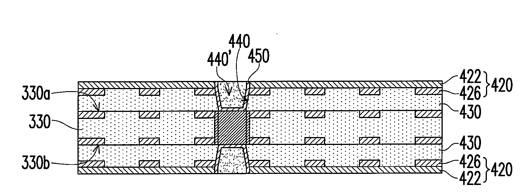
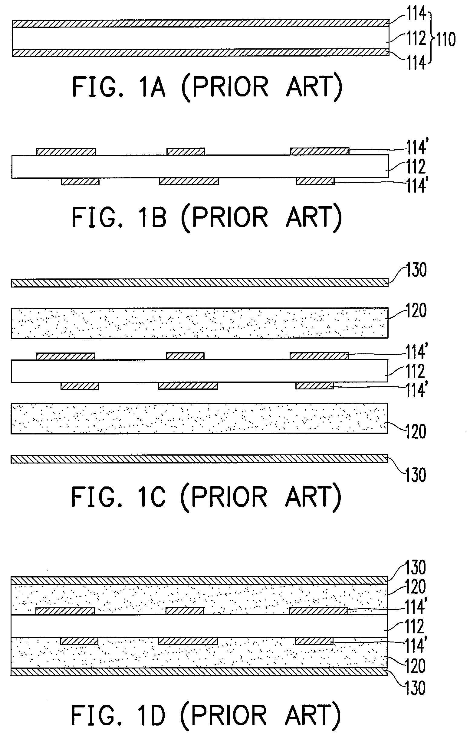
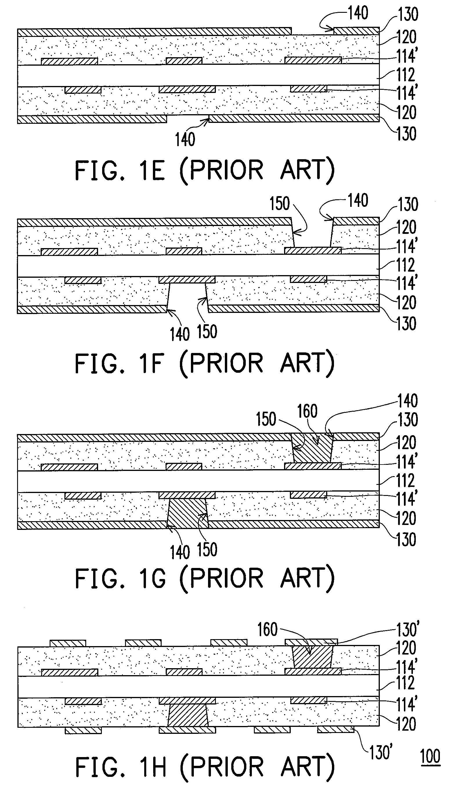
[0031]FIG. 2 is a flowchart illustrating a circuit board process according to an exemplary embodiment of the present invention. Referring to FIG. 2, the circuit board process in the present embodiment includes following steps. First, in step S1, a plurality of first carriers is provided, and a first conductive layer is formed on each of the first carriers, wherein the first conductive layer has a plurality of first concave structures. A first dielectric layer having a first surface and a second surface is then provided in step S2. Next, in step S3, the first carriers with the first conductive layers are laminated on the first and the second surface of the first dielectric layer respectively, wherein ...


PUM

PropertyMeasurementUnit
conductiveaaaaaaaaaa
dielectricaaaaaaaaaa
volumeaaaaaaaaaa

Abstract

A circuit board process is provided. First, multiple carriers is provided, and a first conductive layer having multiple concave structures is formed on each carrier. A dielectric layer is then provided, and the carriers with the first conductive layers are laminated on a first and a second surface of the dielectric layer respectively, wherein portions of the first conductive layers are embedded in the first and second surfaces. Next, the carriers are removed. Thereafter, the first conductive layer corresponding to at least one concave is removed to expose a portion of the dielectric layer. Next, the exposed dielectric layer is removed to form an opening. A second conductive layer is then formed on the inner wall of the opening, wherein the second conductive layer is electrically connected to the first conductive layers on both sides of the dielectric layer.

Description

CROSS-REFERENCE TO RELATED APPLICATION[0001]This application claims the priority benefit of Taiwan application serial no. 96106080, filed Feb. 16, 2007. All disclosure of the Taiwan application is incorporated herein by reference.BACKGROUND OF THE INVENTION[0002]1. Field of the Invention[0003]The present invention generally relates to a circuit board process, and more particularly, to a circuit board process with embedded circuit.[0004]2. Description of Related Art[0005]In recent years, along with the rapid advancement of fabrication techniques in electronic industry, circuit boards can be designed for carrying various small-volume electronic components to be applied to various electronic products. FIGS. 1A˜1H are cross-sectional views illustrating a conventional circuit board process. The conventional circuit board process includes following steps. First, as shown in FIG. 1A, a laminate 110 is provided, wherein the laminate 110 has a core layer 112 and a copper foil layer 114 on ea...

Claims


Application Information

Patent Timeline
Patent Type & Authority Applications(United States)
IPC IPC(8): H01R12/04H05K1/11
CPCH05K3/002Y10T29/49155H05K3/205H05K3/428H05K3/4602H05K3/4658H05K2201/09536H05K2201/09563H05K2201/0959H05K2201/096H05K2203/0554H05K2203/1152Y10T29/49126Y10T29/49156Y10T29/49165Y10T29/49128H05K3/0032
Inventor CHEN, CHUN-CHIENCHEN, TSUNG-YUAN
Owner UNIMICRON TECH CORP
Why Eureka
Try Eureka