Semiconductor device, semiconductor wafer, and electronic device

a semiconductor wafer and semiconductor technology, applied in the direction of solid-state devices, digital storage, instruments, etc., can solve the problems of increasing the on-state current, reducing power consumption cannot be reduced, so as to reduce the reliability of the circuit, increase the on-state current, and reduce the power consumption

Active Publication Date: 2017-09-21
SEMICON ENERGY LAB CO LTD
View PDF7 Cites 8 Cited by
  • Summary
  • Abstract
  • Description
  • Claims
  • Application Information

AI Technical Summary

Benefits of technology

[0010]In a structure of an OS transistor in which a voltage for controlling the threshold voltage is applied to the back gate electrode, a state in which the off-state current is extremely low can be maintained. However, with such a structure, even the current flowing when the transistor is on (on-state current) becomes low. Thus, increasing the on-state current by increasing the driving voltage of the gate electrode becomes necessary. As a result, the following problem arises: the power consumption cannot be reduced. Additionally, in a structure in which the driving voltage of the gate electrode is increased, the electrical characteristics of a transistor might be changed, which might reduce the reliability of the circuit.

Problems solved by technology

However, with such a structure, even the current flowing when the transistor is on (on-state current) becomes low.
As a result, the following problem arises: the power consumption cannot be reduced.
Additionally, in a structure in which the driving voltage of the gate electrode is increased, the electrical characteristics of a transistor might be changed, which might reduce the reliability of the circuit.

Method used


Image

  • Semiconductor device, semiconductor wafer, and electronic device
  • Semiconductor device, semiconductor wafer, and electronic device
  • Semiconductor device, semiconductor wafer, and electronic device

Examples


embodiment 1

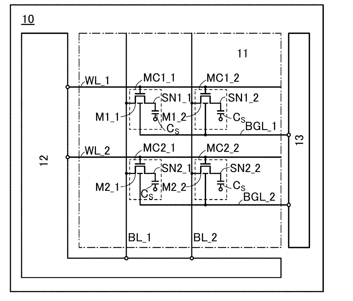
[0049]A structure and an operation of a semiconductor device of one embodiment of the present invention will be described with reference to FIGS. 1A and 1B, FIGS. 2A and 2B, FIGS. 3A and 3B, FIGS. 4A and 4B, FIGS. 5A and 5B, FIG. 6, FIGS. 7A and 7B, FIGS. 8A to 8D, FIG. 9, FIGS. 10A and 10B, FIGS. 11A to 11C, FIGS. 12A to 12E, and FIGS. 13A and 13B. Note that the semiconductor device of one embodiment of the present invention has a function of a memory device capable of retaining data for a certain period of time.

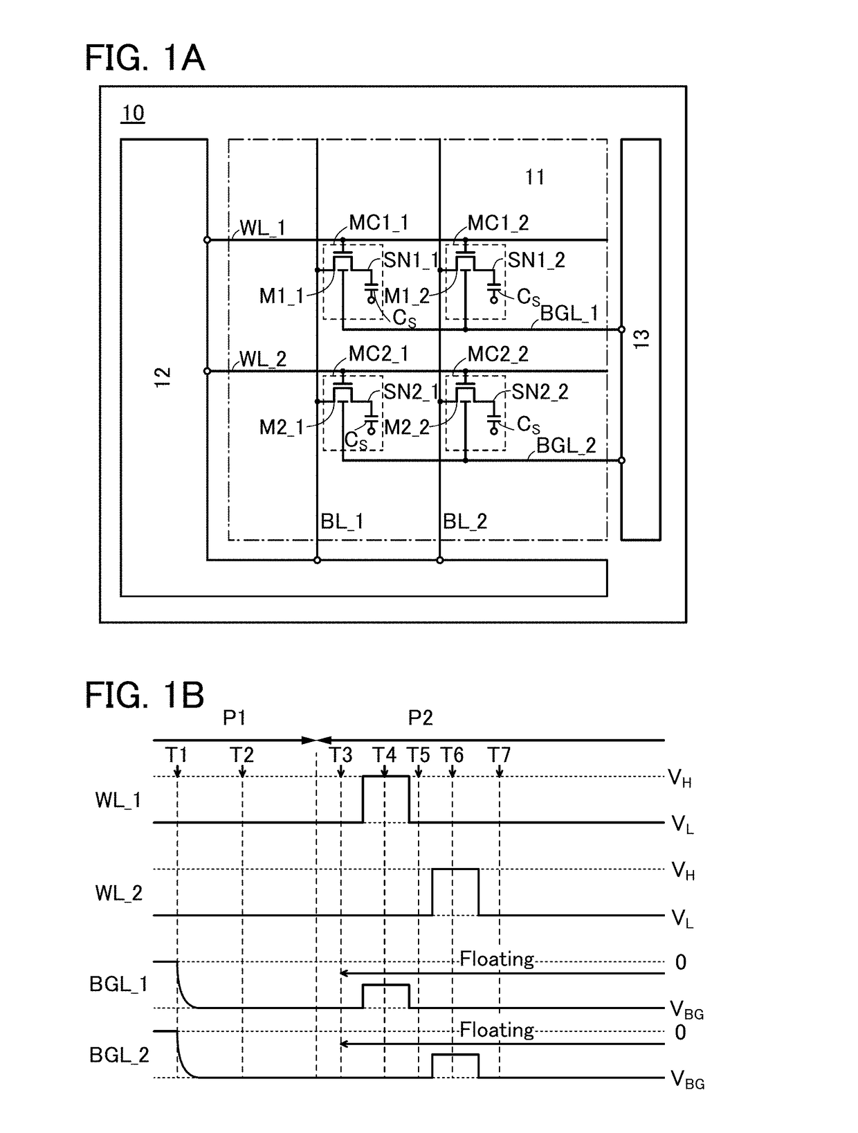
[0050]A semiconductor device 10 shown in FIG. 1A includes a memory cell array 11 (“Memory Cell Array” in the drawing), peripheral circuits 12 (“Peripheral Circuits” in the drawing), and a voltage retention circuit 13 (“VBG Retention Circuit” in the drawing).

[0051]The memory cell array 11 includes, as an example, four memory cells MC (MC1_1, MC1_2, MC2_1, and MC2_2) arranged in two rows and two columns. The number of memory cells MC is not limited to four, and more than four...

modification example

[0103]A modification example of the structure shown in the above-described FIGS. 1A and 1B, FIGS. 2A and 2B, FIGS. 3A and 3B, FIGS. 4A and 4B, FIGS. 5A and 5B, and FIG. 6 will be described with reference to FIGS. 7A and 7B, FIGS. 8A to 8D, FIG. 9, and FIGS. 10A and 10B.

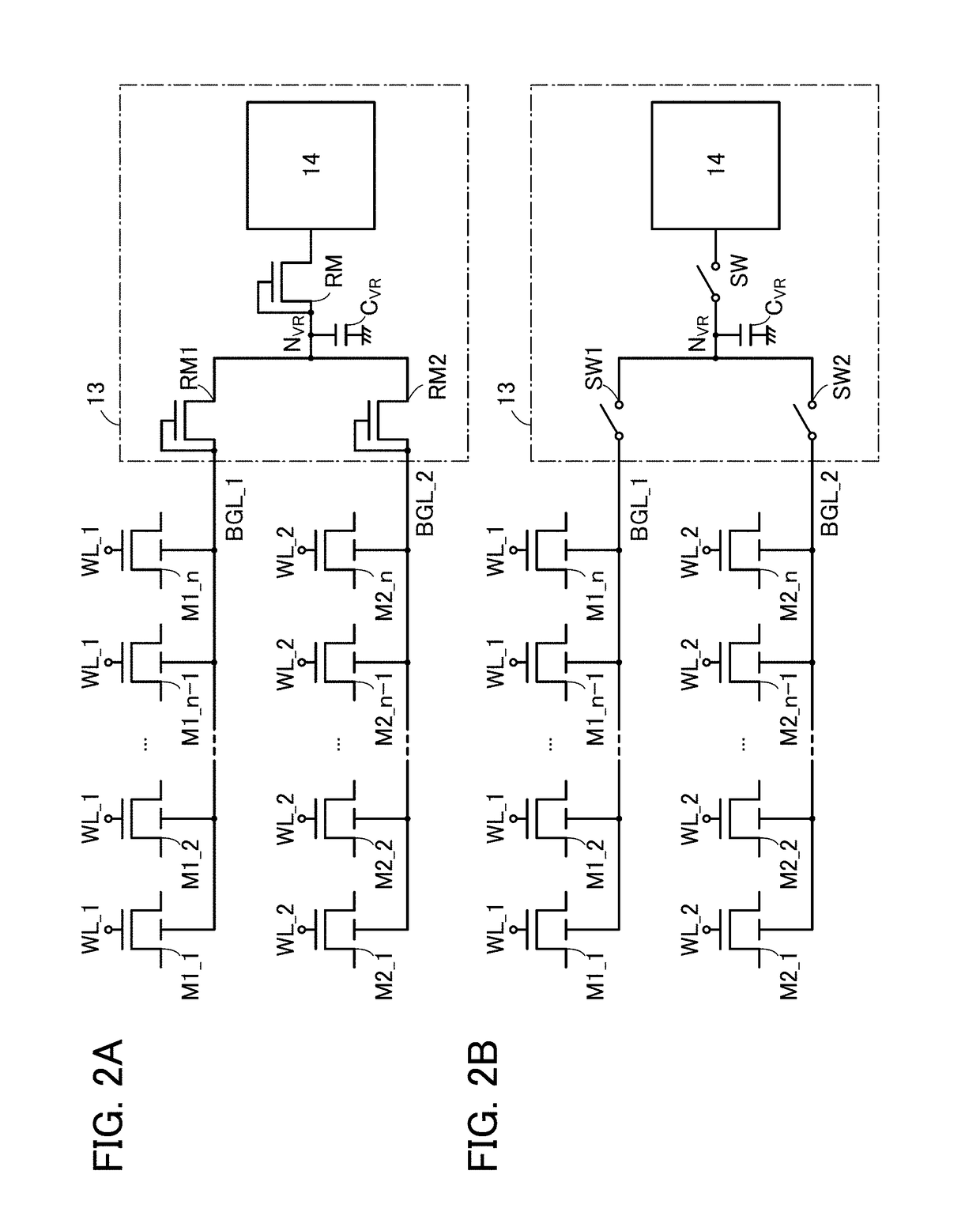
[0104]It is preferable that the back gate lines BGL_1 and BGL_2 shown in FIG. 2A have a large capacitance owing to the capacitor so that a voltage which has been supplied can easily be retained. On the other hand, when the capacitance of the back gate lines BGL_1 and BGL_2 is large, an increase in voltage of the back gate lines due to capacitive coupling between the word line and the back gate line can hardly be achieved. Thus, a structure is preferable in which the capacitor CVR for retaining the voltage of the back gate lines BGL_1 and BGL_2 is provided at the node NVR connected through the transistors RM1 and RM2.

[0105]In order to increase the back gate line by capacitive coupling between the word line and the back...

embodiment 2

[0132]In this embodiment, a structure will be described in which transistors having different electrical characteristics are provided over the same layer. With such a structure, the degree of freedom in design of a semiconductor device can be increased. Additionally, the degree of integration in the semiconductor device can be increased by providing transistors having different electrical characteristics over the same layer.

[0133]As electrical characteristics of the transistor, threshold voltage (Vth) can be given. In this embodiment, structural examples of transistors having different Vth provided over the same layer will be described.

1000>

[0134]FIG. 14A is a cross-sectional view of a semiconductor device 1000. The semiconductor device 1000 includes a transistor 100 and a transistor 200. The transistors 100 and 200 have different structures. FIG. 14A illustrates cross sections of the transistors 100 and 200 over a substrate 101. FIG. 14A corresponds to a cross-sectional view taken ...


PUM


Abstract

A semiconductor device is provided in which the power consumption can be reduced by reducing the driving voltage and the on-state current can be increased in a period in which a transistor having an extremely low off-state current is brought into an electrically floating state. The semiconductor device comprises a memory cell, a first circuit, and a second circuit. The memory cell includes a first transistor. The first transistor includes a first semiconductor layer, a first gate electrode, and a first back gate electrode. The first gate electrode is connected to a word line. The first back gate electrode is connected to a back gate line. The first circuit supplies a signal for controlling the conduction state of the first transistor to the word line. The second circuit supplies a voltage for controlling the threshold voltage of the first transistor to the back gate line. The second circuit has a function of bringing the back gate line into an electrically floating state in a period in which a signal for controlling the conduction state of the first transistor is supplied to the word line.

Description

BACKGROUND OF THE INVENTION[0001]1. Field of the Invention[0002]One embodiment of the present invention relates to a semiconductor device, a semiconductor wafer, and an electronic device.[0003]Note that one embodiment of the present invention is not limited to the above technical field. One embodiment of the invention disclosed in this specification and the like relates to an object, a method, or a manufacturing method. Furthermore, one embodiment of the present invention relates to a process, a machine, manufacture, or a composition of matter.[0004]In this specification and the like, a semiconductor device generally means a device that can function by utilizing semiconductor characteristics. A display device (e.g., a liquid crystal display device and a light-emitting display device), a projection device, a lighting device, an electro-optical device, a power storage device, a memory device, a semiconductor circuit, an imaging device, an electronic device, and the like may include a ...

Claims


Application Information

Patent Timeline
Patent Type & Authority Applications(United States)
IPC IPC(8): H01L29/786G11C16/04H01L27/11563H01L29/24H01L27/11517
CPCH01L29/7869H01L29/24G11C16/0466H01L27/11563G11C16/0416H01L27/11517G11C16/0433G11C2213/79G11C11/401G11C11/404H01L27/1225H01L27/1255G11C11/4074G11C11/403H01L29/78648H10B41/00H10B43/00
Inventor ONUKI, TATSUYAKATO, KIYOSHIATSUMI, TOMOAKI
Owner SEMICON ENERGY LAB CO LTD
Why Eureka
Try Eureka