Method for fabricating conductive blind via of circuit substrate

Active Publication Date: 2007-07-19
ADVANCED SEMICON ENG INC
View PDF4 Cites 8 Cited by
  • Summary
  • Abstract
  • Description
  • Claims
  • Application Information

AI Technical Summary

Benefits of technology

[0009]The invention is directed to a method for fabricating a conductive blind

Problems solved by technology

Therefore, a portion of the electroless copper layer contacting the capture pad flakes off easily due to thermal stress generated when the circuit substrate is functioning.
A bad con

Method used


Image

  • Method for fabricating conductive blind via of circuit substrate
  • Method for fabricating conductive blind via of circuit substrate
  • Method for fabricating conductive blind via of circuit substrate

Examples


Example

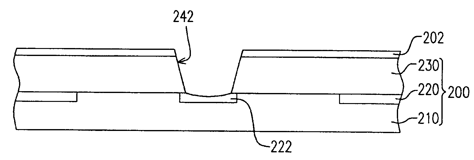
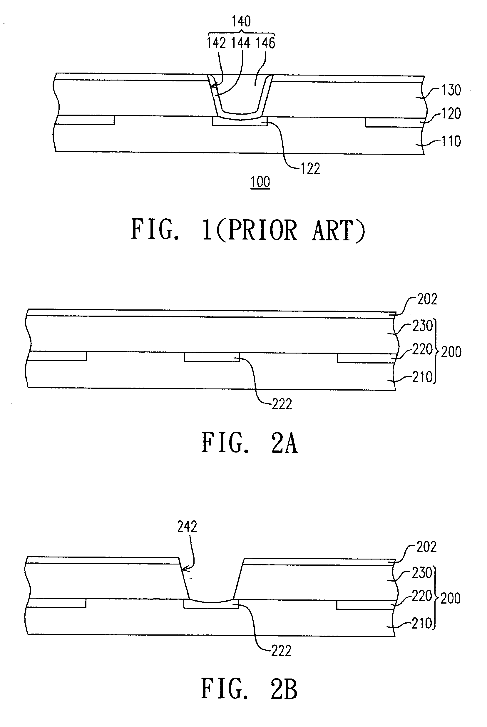
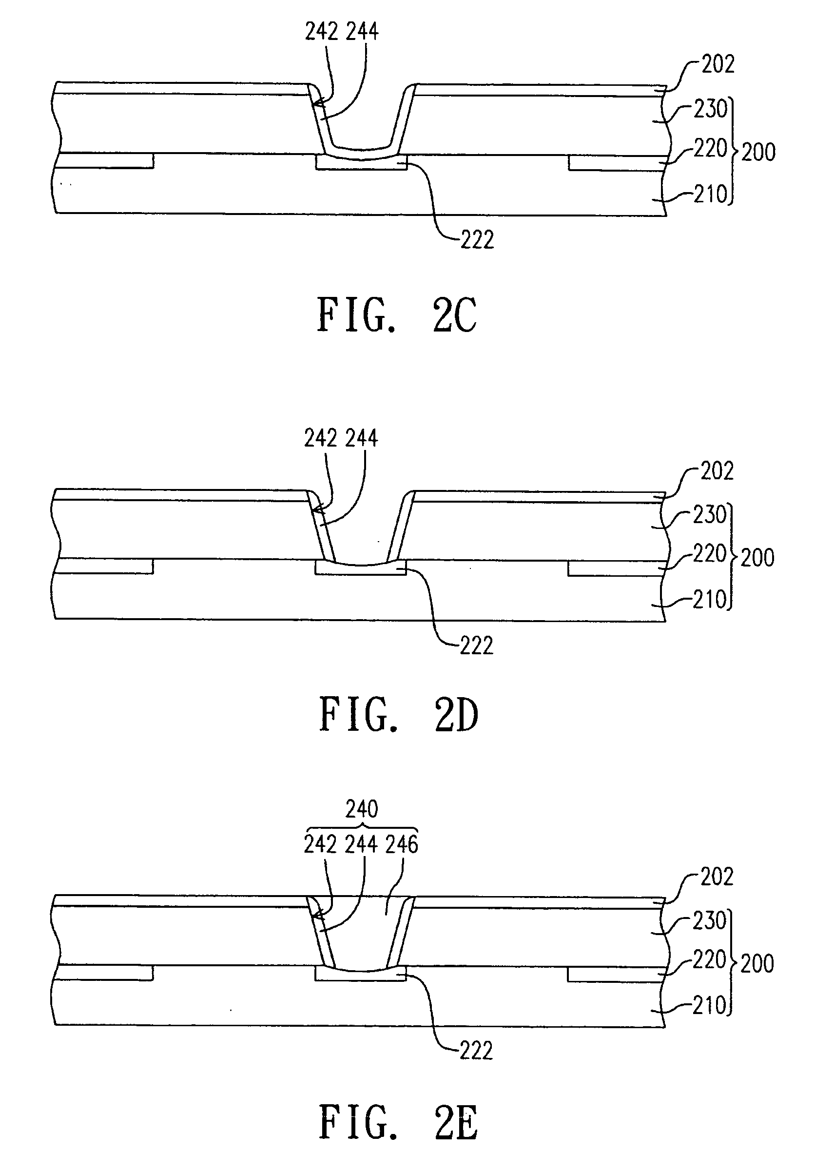
[0027]FIGS. 2A˜2E illustrates cross-sectional views of a method for fabricating a conductive blind via of a circuit substrate according to a preferred embodiment of the invention. The method includes following steps. First, as shown in FIG. 2A, a circuit substrate 200 is provided. The circuit substrate 200 includes a first dielectric layer 210, a patterned circuit layer 220 and a second dielectric layer 230. The patterned circuit layer 220 is disposed between the first dielectric layer 210 and the second dielectric layer 230. The first dielectric layer 210 is a core layer for example. The patterned circuit layer 220 in the present embodiment preferably includes one or more capture pads 222 (one capture pad 222 illustrated in FIG. 2A as an example). The capture pad 222 is preferably made of copper. In an embodiment, a metal circuit layer 202 is disposed on the second dielectric layer 230. Preferably, the metal circuit layer 202 is electrically connected to the patterned circuit layer...


PUM

PropertyMeasurementUnit
Dielectric polarization enthalpyaaaaaaaaaa
Electrical conductoraaaaaaaaaa

Abstract

A method for fabricating a conductive blind via of a circuit substrate including the following steps is provided. First, the circuit substrate including a first dielectric layer, a patterned circuit layer and a second dielectric layer are provided. The patterned circuit layer including at least a capture pad is disposed between the first dielectric layer and the second dielectric layer. Next, a blind via exposing the capture pad is formed in the second dielectric layer. Then, an electroless plating process is performed to form an electroless copper layer on the capture pad and an inner wall of the blind via. Next, the electroless copper layer on the capture pad is removed. Finally, the blind via is filled with a conductive material to form the conductive blind via.

Description

[0001]This application claims the benefit of Taiwan application Serial No. 95101551, filed Jan. 16, 2006, the subject matter of which is incorporated herein by reference.BACKGROUND OF THE INVENTION[0002]1. Field of the Invention[0003]The invention relates in general to a method for fabricating a circuit substrate, and more particularly to a method for fabricating a conductive blind via of a circuit substrate.[0004]2. Description of the Related Art[0005]Circuit substrates are formed by stacking several dielectric layers and several patterned circuit layers alternately. The patterned circuit layers are defined by lithography and etching a copper layer. The dielectric layers are disposed between the patterned circuit layers for protecting and separating the patterned circuit layers. The patterned circuit layers are electrically connected to each other through conductive blind vias in the dielectric layers. Furthermore, several contacts are formed on surfaces of the circuit substrates f...

Claims


Application Information

Patent Timeline
IPC IPC(8): H01K3/10C25D5/02
CPCC23C18/1603C25D5/02C25D5/34H05K3/027H05K3/421H05K2203/0353Y10T29/49163C23C18/1653C23C18/1689C23C18/38Y10T29/49165Y10T29/49156H05K2203/0361
Inventor WANG, TE-CHUN
Owner ADVANCED SEMICON ENG INC
Why Eureka
Try Eureka