Method for forming ball pads of BGA substrate

Inactive Publication Date: 2005-03-10
ADVANCED SEMICON ENG INC
View PDF13 Cites 27 Cited by
  • Summary
  • Abstract
  • Description
  • Claims
  • Application Information

AI Technical Summary

Benefits of technology

[0005] The main purpose of the present invention is to provide a method for forming ball pads of a BGA substrate. A substrate with a plurality of pad terminals is provided and a solder mask is coated on the substrate. After solder mask processing step, a metal layer for redefining ball pads is

Problems solved by technology

However, the bonding strength from NSMD ball pads to the substrate and solder balls are poor.
However, solder balls contact the solder mask openings on the SMD ball pads, the bonding strength from the SMD ball pads to solder balls is poor.
Moreover, the SMD ball pads occupy a larger area of the ball-placement surface of the substrate, the wirings cannot be formed in high density.
The stress from the solder mask 120 will directly be focused on the solder balls 150, eventually, the re

Method used


Image

  • Method for forming ball pads of BGA substrate
  • Method for forming ball pads of BGA substrate
  • Method for forming ball pads of BGA substrate

Examples


Embodiment Construction

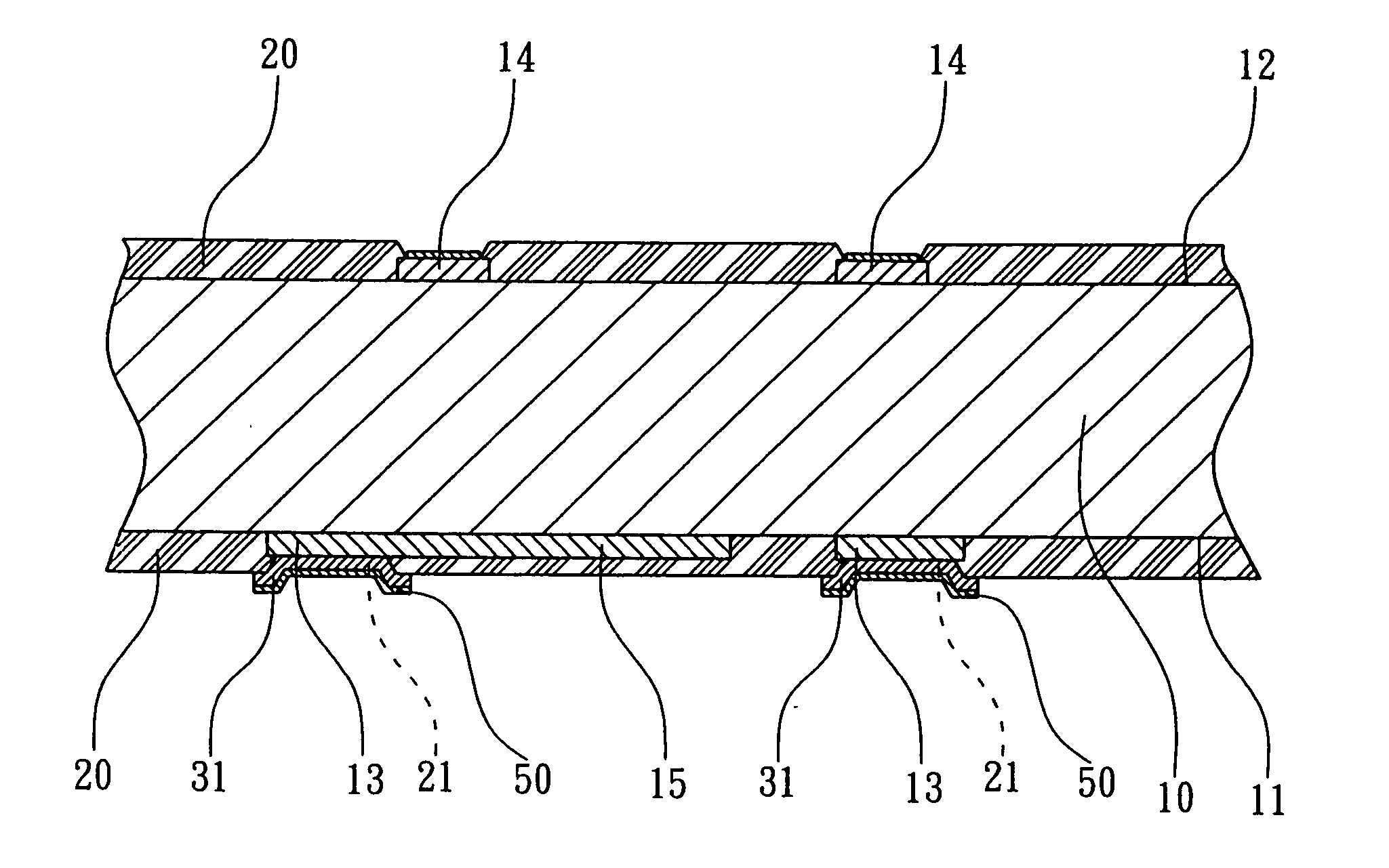
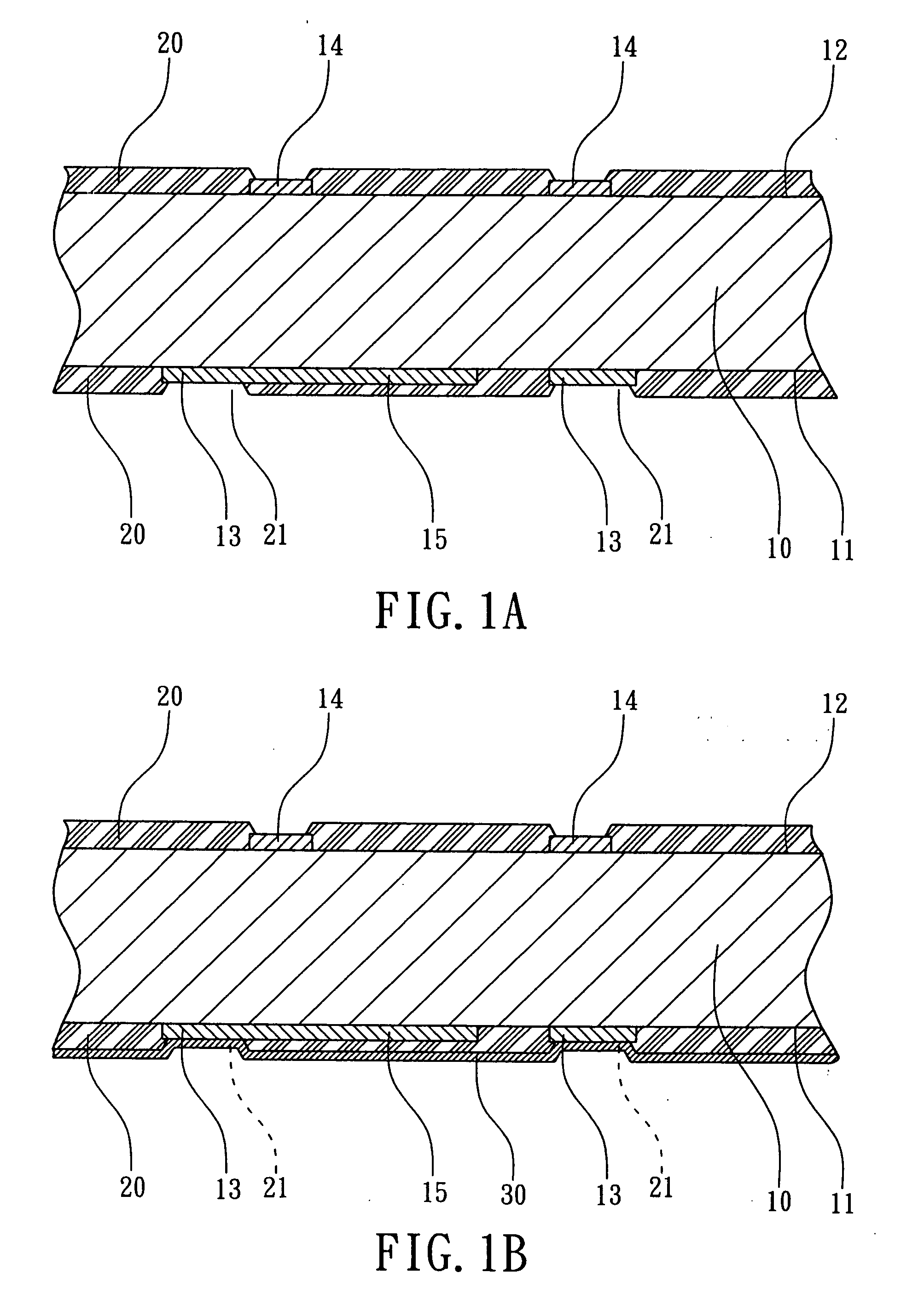
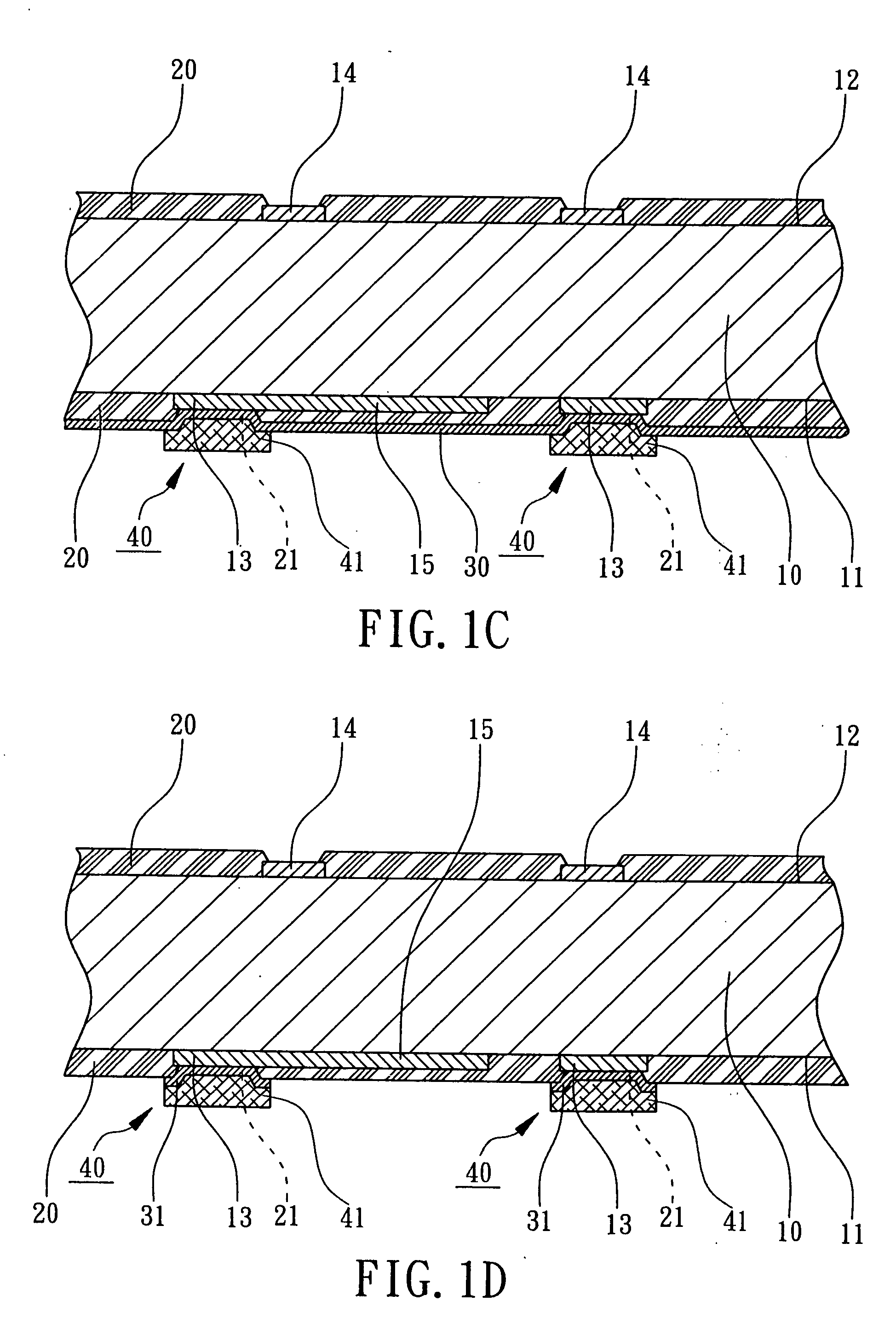
[0014] Please refer to the drawings attached, the present invention is described by means of an embodiment below. According to the present invention, the process for forming balls pads of a BGA substrate is disclosed. Referring to FIG. 1A, firstly, a substrate 10 is provided, which has a ball placement surface 11 and a die-attach surface 12 for attaching a semiconductor chip 60 (as shown in FIG. 3). A plurality of bonding pads 14 are formed on the die-attach surface 12 for electrical connection to the chip 60. A plurality of pad terminals 13 are formed on the surface 11. And solder masks 20 are formed on the surface 11 and the die-attach surface 12 respectively. As shown in FIG. 1A, the pad terminals 13 are fabricated from a same wiring layer including a plurality of metal wirings 15 on the surface 11 of the substrate 10. The pad terminals 13 can be in various shapes selected from square pads, or circular pads, even a trace terminal. As shown in FIG. 2, in this embodiment the pad te...


PUM


Abstract

A method for forming ball pads of a BGA substrate is disclosed. A substrate is provided with a plurality of pad terminals on its surface. A solder mask is formed on the surface and has a plurality of openings to expose the pad terminals. A metal layer for redefining ball pads is formed on the solder mask. An etching mask is formed on the metal layer, the etching mask has a plurality of covering portions which are aligned with the pad terminals and larger than the openings of the solder mask. The metal layer is etched to form a plurality of redefined ball pads under the etching mask. The redefined ball pads cover the pad terminals of the substrate and extend around the openings of the solder mask so that solder balls can be jointed with the redefined ball pads to avoid contacting the solder mask and the pad terminals by redefinition of bonding area of solder balls.

Description

FIELD OF THE INVENTION [0001] The present invention relates to a method for fabricating a BGA (ball grid array) substrate, more particularly, to a method for forming ball pads of a BGA substrate. BACKGROUND OF THE INVENTION [0002] Conventionally, a ball grid array (BGA) substrate provides a chip carrier for BGA package. The BGA substrate includes a plurality of ball pads which are made by laminating a copper foil and then etching the copper foil to form the ball pads. The ball pads are configured for solder ball placement to provide outer electrical connection of BGA packages. Normally, a solder mask is applied on the BGA substrate to cover the corresponding circuits and expose the ball pads. The formation of the solder mask is a final step after the fabrication of the ball pads. According to the design of the openings of the solder mask, the ball pads can be classified into Non Solder Mask Defined (NSMD) pads and Solder Mask Defined (SMD) pads. On one hand, the NSMD ball pads are s...

Claims


Application Information

Patent Timeline
IPC IPC(8): H01L21/48H01L23/498H05K1/11H05K3/06H05K3/34H05K3/42
CPCH01L21/4853H01L24/48H01L2224/48091H01L2224/48227H05K1/111H05K1/112H05K3/061H05K3/062H05K3/3484H05K3/421H05K2201/09436H05K2201/09509H05K2201/0969H05K2203/054H01L23/49816H01L2924/00014H01L2924/181H05K3/3485H01L2924/00012H01L2224/45099H01L2224/45015H01L2924/207
Inventor DING, YI-CHUANKO, SHUN-FU
Owner ADVANCED SEMICON ENG INC
Why Eureka
Try Eureka