Method of fabricating a dual damascene interconnect structure

a technology of damascene and interconnect structure, which is applied in the direction of surface treatment compositions, decorative arts, chemistry apparatus and processes, etc., can solve the problems of suboptimal or non-optimal operation of the interconnect structure, material eroded, cracked or peeling off, and the position of the contact hole and the trench

Inactive Publication Date: 2006-10-03
APPLIED MATERIALS INC
View PDF10 Cites 32 Cited by
  • Summary
  • Abstract
  • Description
  • Claims
  • Application Information

AI Technical Summary

Benefits of technology

[0010]The present invention is a method of fabricating an interconnect structure (e.g., dual damascene interconnect structure, and the like) of an integrated circuit device. The interconnect structure is fabricated using a bi-layer mask comprising an imaging layer (e.g., a photoresist film or a silicon-rich photoresist film) and an organic planarizing film. The bi-layer mask removes lithographic misalignment between a contact hole, a trench, and an underlying conductive line when the interconnect structure is formed. Additionally, a sacrificial layer may be used to protect an inter-metal dielectric (IMD) layer during subsequent planarization of the interconnect structure. The sacrificial layer may be formed of a dielectric material (e.g., amorphous silicon (Si), and the like) or a metallic layer (e.g., titanium nitride (TiN), tungsten (W), and the like). The interconnect structure may be formed of a metal (e.g., copper (Cu), aluminum (Al), tantalum (Ta), tungsten (W), titanium (Ti), and the like) or a conductive compound (e.g., tantalum nitride (TaN), titanium nitride (TiN), tungsten nitride (WN), and the like).

Problems solved by technology

During fabrication of the interconnect structure, lithographic errors may result in misalignment between the positions of a contact hole and a trench of the structure.
Additionally, mechanical stress, as well as chemically aggressive agents used during the planarization process, may cause the material of the IMD layer to erode, crack, or peel off.
Such defects may render the interconnect structure to operate sub-optimally or not at all.

Method used


Image

  • Method of fabricating a dual damascene interconnect structure
  • Method of fabricating a dual damascene interconnect structure
  • Method of fabricating a dual damascene interconnect structure

Examples


Embodiment Construction

[0019]The present invention is a method of fabricating an interconnect structure on a substrate (e.g., a silicon (Si) wafer) using a bi-layer mask to pattern a contact hole or a trench in an inter-metal dielectric (IMD) layer of the interconnect structure. The method additionally removes lithographic misalignment between the contact hole, the trench, and an underlying conductive line. In one embodiment, the invention is used to fabricate a dual damascene copper interconnect structure.

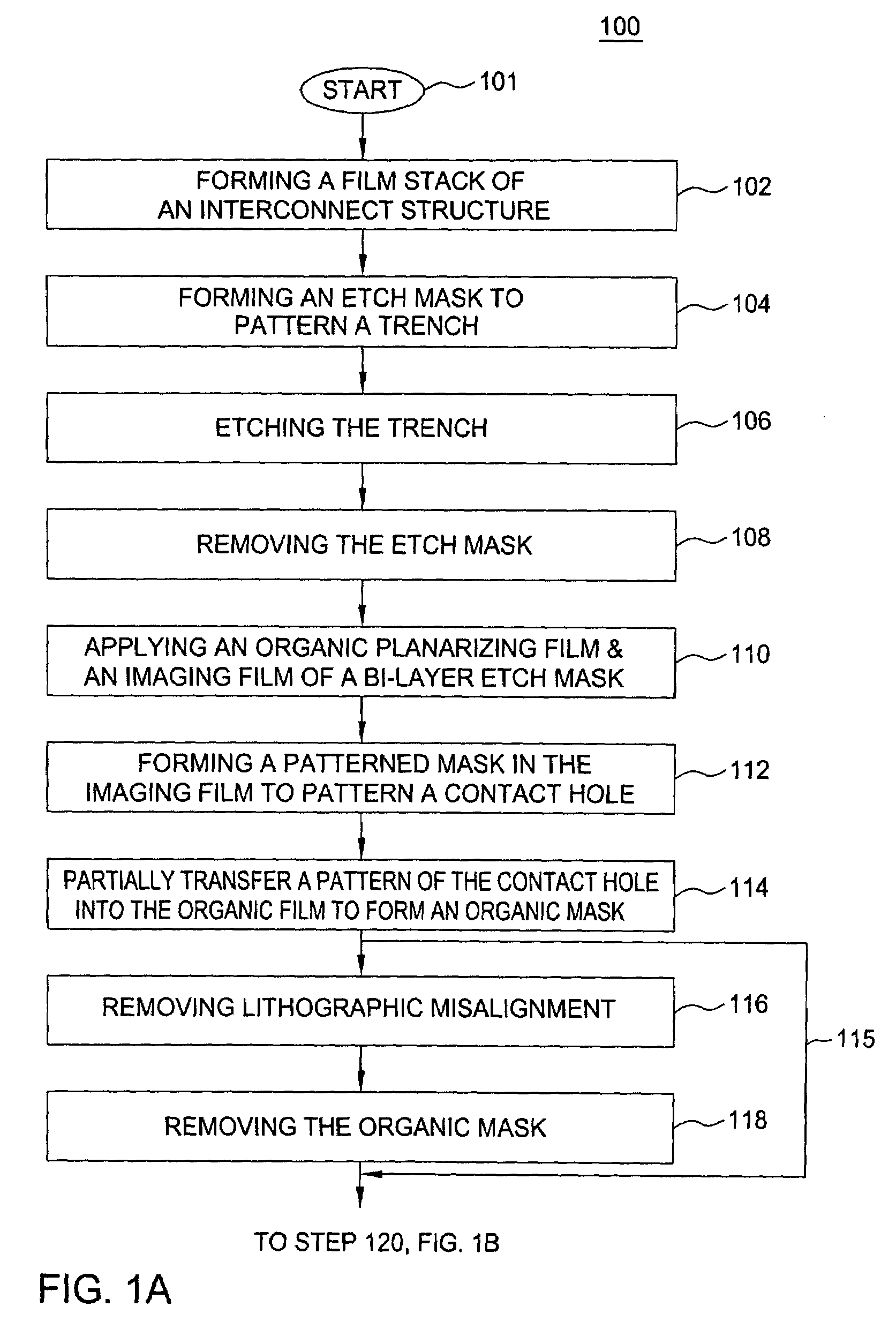
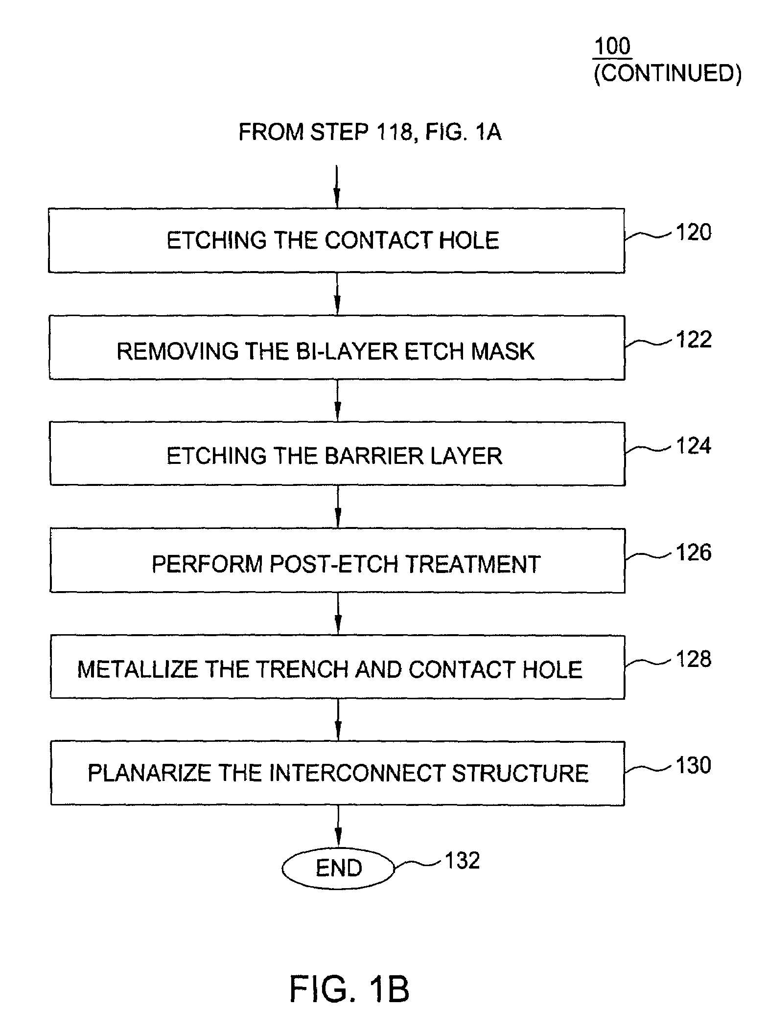
[0020]FIGS. 1A–1B depict a flow diagram of one embodiment of the inventive method for fabricating a dual damascene interconnect structure as a sequence 100. The sequence 100 comprises the processes that are performed upon a film stack during fabrication of the dual damascene interconnect structure.

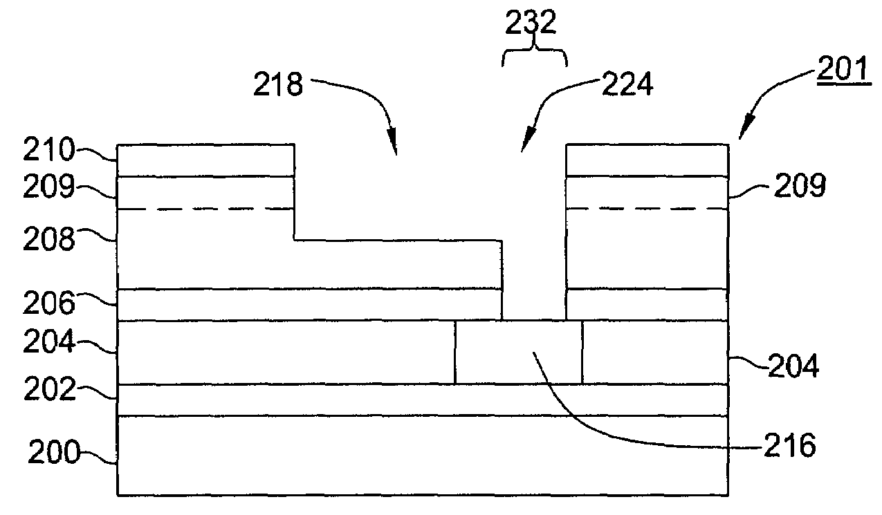
[0021]FIGS. 2A–2N depict a sequence of schematic, cross-sectional views of a substrate having a dual damascene interconnect structure being fabricated using the sequence 100. The cross-sectional views in FIGS....


PUM

PropertyMeasurementUnit
dielectric constantsaaaaaaaaaa
thicknessaaaaaaaaaa
dielectric constantaaaaaaaaaa

Abstract

A method of fabricating an interconnect structure (e.g., dual damascene interconnect structure, and the like) of an integrated circuit device is disclosed. The interconnect structure is fabricated using a bi-layer mask comprising an imaging film and an organic planarizing film. The bi-layer mask is used to remove lithographic misalignment between a contact hole, a trench, and an underlying conductive line when the interconnect structure is formed. Additionally, a sacrificial layer may be used to protect an inter-metal dielectric (IMD) layer during subsequent planarization of the interconnect structure. The sacrificial layer may be formed of amorphous silicon (Si), titanium nitride (TiN), tungsten (W), and the like. The interconnect structure may be formed of a metal (e.g., copper (Cu), aluminum (Al), tantalum (Ti), tungsten (W), titanium (Ti), and the like) or a conductive compound (e.g., tantalum nitride (TaN), titanium nitride (TiN), tungsten nitride (WN), and the like).

Description

CROSS REFERENCE TO RELATED APPLICATIONS[0001]This application claims benefit of U.S. provisional application Ser. No. 60 / 460,940, filed Apr. 7, 2003, which is herein incorporated by reference.BACKGROUND OF THE INVENTION[0002]1. Field of the Invention[0003]The present invention generally relates to fabrication of semiconductor integrated circuits. More specifically, the present invention relates to a method of fabricating interconnect structures in a semiconductor substrate processing system.[0004]2. Description of the Related Art[0005]Integrated circuits (IC) are manufactured by forming discrete semiconductor devices on a surface of a semiconductor substrate, such as a silicon (Si) wafer. A multi-level network of interconnect structures is then formed to interconnect the devices. Copper (Cu) is the wiring material of choice for interconnect structures of advanced IC devices having a high circuit density. In addition to superior electrical conductivity, copper is more resistant than ...

Claims


Application Information

Patent Timeline
Patent Type & Authority Patents(United States)
IPC IPC(8): H01L21/302H01L21/3065H01L21/027H01L21/033H01L21/311H01L21/768
CPCH01L21/31144H01L21/76801H01L21/76808H01L21/7684H01L21/0274H01L21/0332
Inventor YE, YANZHAO, XIAOYEDU, HONG
Owner APPLIED MATERIALS INC
Why Eureka
Try Eureka