
Planar lighting device

a lighting device and planar technology, applied in the direction of lighting device details, lighting and heating equipment, instruments, etc., can solve the problems of inability to reduce the distance that light can travel limits the extent to which the dimensions of the planar lighting device can be increased, and the thickness and weight of the planar lighting device cannot be reduced. , to achieve the effect of reducing the thickness and weight of the planar lighting device, increasing the dimension

Active Publication Date: 2010-08-10
FUJIFILM CORP
View PDF24 Cites 39 Cited by
  • Summary
  • Abstract
  • Description
  • Claims
  • Application Information

AI Technical Summary

Benefits of technology

[0014]Further, to achieve increased dimensions with a planar lighting device using any of the light guide plates disclosed in the above prior art literature, light needs to travel a longer distance from the light source, which in turn requires the light guide plate itself to be made thicker. Thus, there still remains a problem that it is impossible to reduce thickness and weight of the planar lighting device.
[0017]Thus, an object of the present invention is to provide a planar lighting device that eliminates problems accompanying the above prior art, ensures that the light emitted through the light exit plane represents a high-in-the-middle, bell-curve illuminance distribution without increasing the number of light sources and manufacturing costs while keeping power consumption at low levels, and achieves a thinner design and greater dimensions, thus making the planar lighting device suitable for applications in liquid crystal display devices such as liquid crystal televisions.
[0043]The above configuration according to the invention ensures that the light emitted through the light exit plane represents a high-in-the-middle, bell-curve illuminance distribution without increasing the number of light sources and manufacturing costs while keeping power consumption at low levels, by admitting through a pair of light entrance planes light having a light amount distribution varying or an amount distribution of light that is different in the longitudinal direction of each of a pair of light entrance planes, which is accomplished by, for example, arraying LED chips at a varying array density or arraying LED chips having different light amounts.
[0044]In particular, according to a first aspect of the invention, the number of LED chips can be reduced by disposing LED chips at a varying array density. This in turn reduces the manufacturing costs and power consumption of the device.
[0045]Further, according to a second aspect of the invention, LED chips comprising LEDs producing a low light amount can be used. This reduces the manufacturing costs and power consumption of the device.

Problems solved by technology

Thus, there still remains a problem that it is impossible to reduce thickness and weight of the planar lighting device.
Further, the shape having a tendency to decrease in thickness with the increasing distance from a position at which light from the light source is admitted or the flat plate shape as disclosed in the prior art literature mentioned above also pose a problem that a limited distance that light is capable of traveling limits the extent to which the dimensions of the planar lighting device can be increased.
While use of a light source having large light emission faces and hence providing more light to the light guide plate would enable emission of light with an increased brightness or an increased illuminance through the light exit plane, that approach is accompanied by a problem that there is a limit to the dimensions of the light emission face of the light source that can be used depending on the configuration of the light guide plate.
Besides, use of a larger light source or a light source providing a greater amount of light would increase the manufacturing costs of the device and power consumption thereof.

Method used


Image

  • Planar lighting device
  • Planar lighting device
  • Planar lighting device

Examples


Embodiment Construction

[0062]The planar lighting device of the invention will be described in detail below referring to an embodiment illustrated in the accompanying drawings.

[0063]Now, a first example of the invention will be described first.

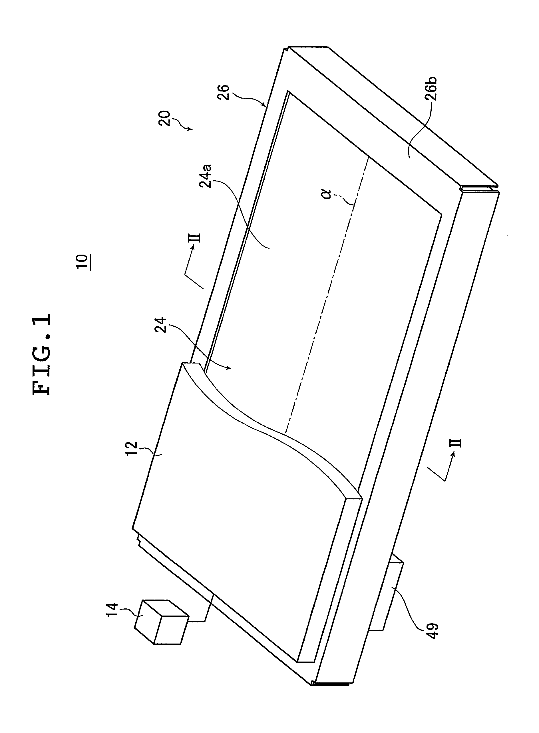
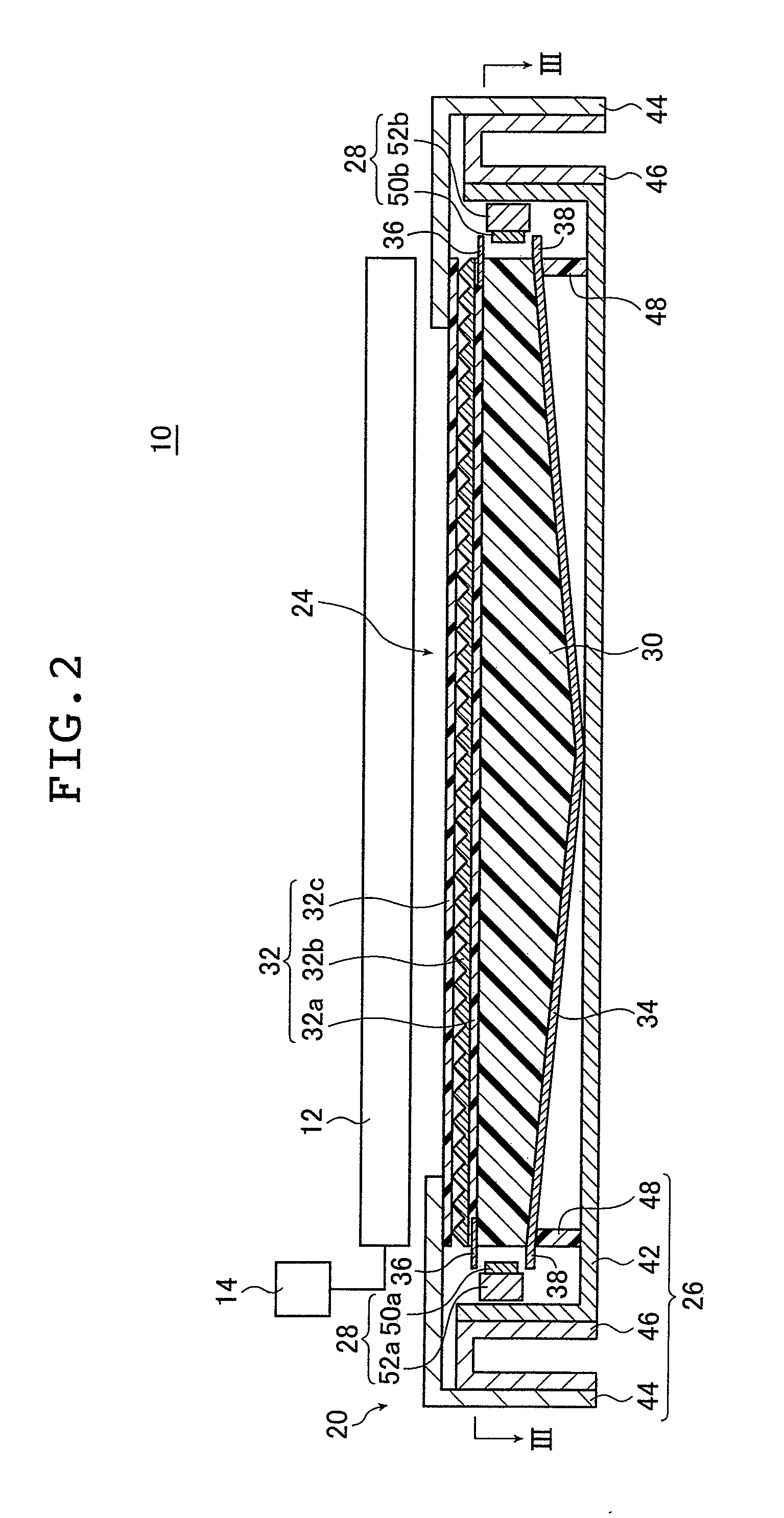
[0064]FIG. 1 is a schematic perspective view illustrating a liquid crystal display device provided with the planar lighting device of the invention; FIG. 2 is a cross sectional view of the liquid crystal display device illustrated in FIG. 1 taken along line II-II.

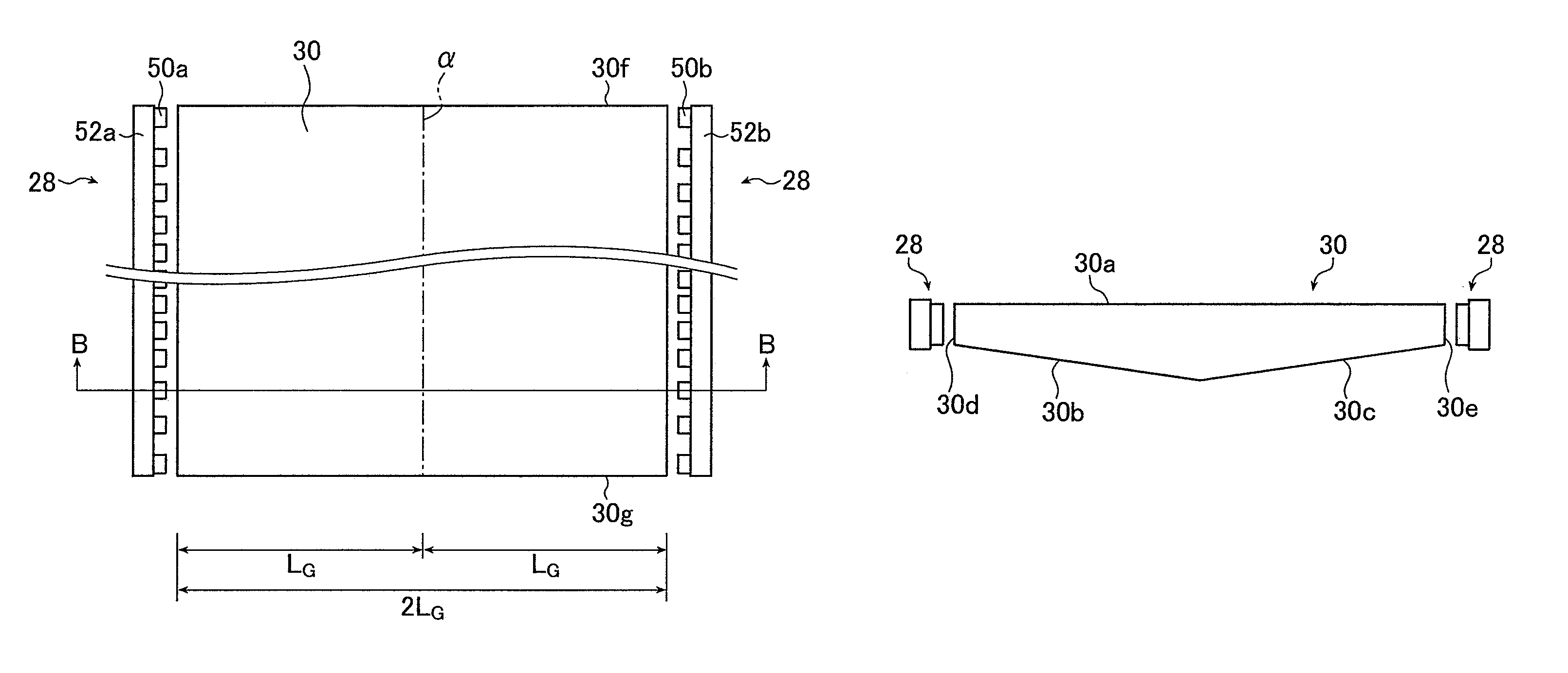
[0065]FIG. 3A is a view of the planar lighting device (also referred to as “backlight unit” below) illustrated in FIG. 2 taken along line III-III; FIG. 3B is a cross sectional view of FIG. 3A taken along line B-B.

[0066]A liquid crystal display device 10 comprises a backlight unit 20, a liquid crystal display panel 12 disposed on the side of the backlight unit closer to the light exit plane, and a drive unit 14 for driving the liquid crystal display panel 12. In FIG. 1, part of the liquid crystal display pane...


PUM


Abstract

A thinner and larger planar lighting device is achieved without increasing the number of light sources and holding the power consumption to a minimum. The LED chips on the light sources are arrayed at an array density varying according to the position of each of the light entrance planes of the light guide plate such that the illuminance distribution as measured on along the middle of the light guide plate in a direction parallel to longitudinal direction of the light entrance planes represents a high-in-the-middle, bell-curve distribution.

Description

[0001]The entire contents of literature cited in this specification are incorporated herein by reference.BACKGROUND OF THE INVENTION[0002]The present invention relates to a planar lighting device comprising light sources and a light guide plate for admitting light emitted by the light sources and emitting the light through the light exit plane thereof. The inventive planar lighting device is used for indoor and outdoor illumination or as a backlight to illuminate the liquid crystal display panel used in liquid crystal display devices or a backlight used for advertising panels, advertising towers, advertising signs, and the like.[0003]Liquid crystal display devices use a backlight unit for radiating light from behind the liquid crystal display panel to illuminate the liquid crystal display panel. A backlight unit is configured using optical members comprising a light guide plate for diffusing light emitted by an illuminating light source to irradiate the liquid crystal display panel,...

Claims


Application Information

Patent Timeline
Patent Type & Authority Patents(United States)
IPC IPC(8): F21V7/04
CPCG02B6/0041G02B6/0046G02B6/0068G02B6/0073
Inventor IWASAKI, OSAMU
Owner FUJIFILM CORP
Learn More