Method and apparatus for correcting errors of a photolithographic mask

a photolithographic mask and error correction technology, applied in the field of photolithographic mask error correction, can solve the problems of increasing the complexity of photolithographic mask manufacturing, and increasing the cost of photoresist variations, so as to reduce the overlay error and reduce the remaining registration error

Active Publication Date: 2012-01-12
CARL ZEISS SMS GMBH
View PDF10 Cites 85 Cited by
  • Summary
  • Abstract
  • Description
  • Claims
  • Application Information

AI Technical Summary

Benefits of technology

[0016]The simultaneous variation of the imaging parameters and of the laser beam parameters expands the dimension of the variation space of the optimization process compared to the step-wise optimization according to the prior art. The expanded solution space in a joint optimization process for the imaging parameters and the laser beam parameters results in a reduction of the overall error of photolithographic masks not attainable with prior art optimization processes. Thus, the application of the defined error correction method will significantly increase the yield of the mask fabrication process.
[0067]For the fabrication of a semiconductor device normally a series of photolithographic masks is successively applied on the same wafer during the manufacturing process in order to generate complex structures on the wafer. In many applications the absolute location of the mask pattern with respect to the optical axis is not as important as the orientation of two or more masks relative to each other so that overlay critical structures can be printed onto the wafer. So the target is not to bring a first photolithographic mask to the best match with a predetermined design, but to obtain the best match with a second mask. The inventive method can also be used to correct such overlay errors of two or more photolithographic masks. In particular, if the first and the second parameters of both masks can simultaneously be varied the relative orientation of the two masks can be optimized with a low remaining registration error.

Problems solved by technology

As a consequence, the manufacturing of photolithographic masks with increasing resolution is becoming more and more complex, and thus more and more expensive as well.
Larger deviations of the planarity of the substrate of the photolithographic mask may lead to variations of the optical intensity distribution in the photoresist due to a constructive of a destructive addition of the wave front in the photoresist.
At the further processing of the wafer, the variations of the optical intensity may result in the fabrication of defective semiconductor devices.
Decreasing exposure wavelength makes this problem more challenging.
The substrate as supplied from the manufacturer may not even fulfil the planarity condition for EUV photolithographic masks and the manufacturing process of the mask which forms fine patterns on one surface may even deteriorate the planarity of the substrate.
Furthermore, a curvature of the substrate of a photolithographic mask also leads to imaging errors of the mask.
In addition to errors introduced due to diffraction at the pattern elements, the pattern elements forming the photolithographic mask may also be defective.
Moreover, photolithographic masks may also have placement errors of pattern elements, i.e. some of the pattern elements do not image the pattern parameters exactly at the predetermined position on the photoresist.
However, this approach still retains an amount of errors of a photolithographic mask which can in many cases not be tolerated.

Method used


Image

  • Method and apparatus for correcting errors of a photolithographic mask
  • Method and apparatus for correcting errors of a photolithographic mask
  • Method and apparatus for correcting errors of a photolithographic mask

Examples


Embodiment Construction

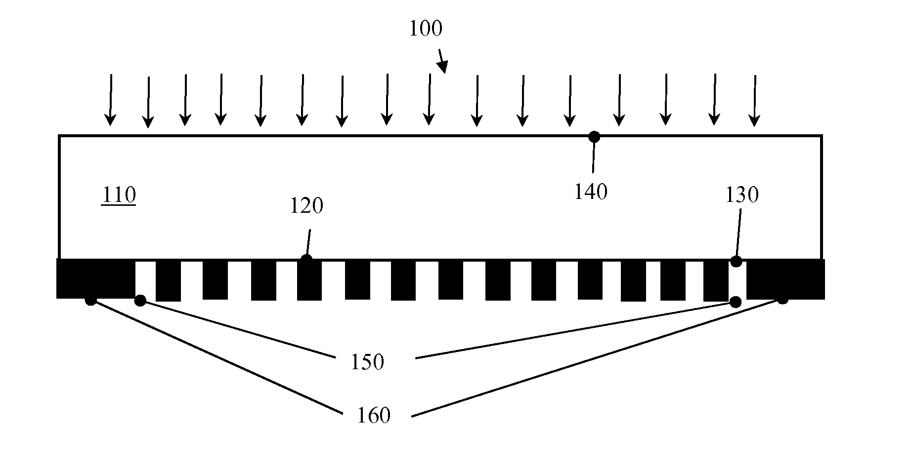
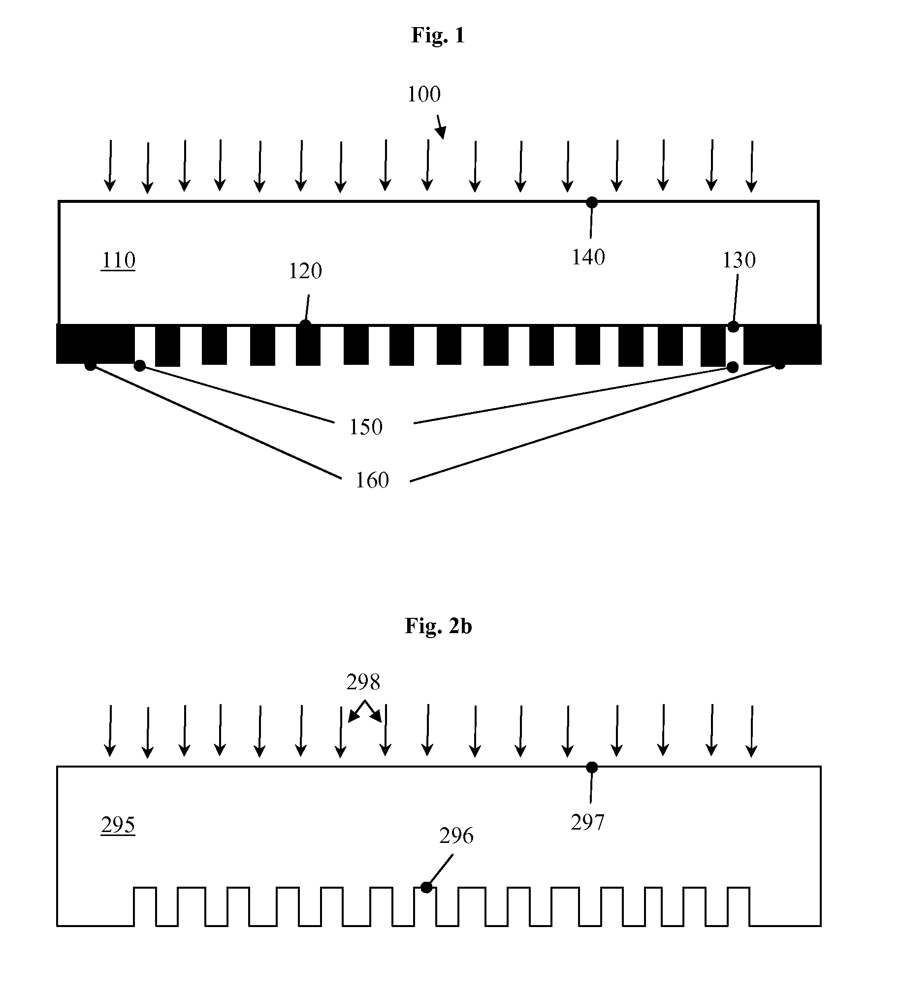
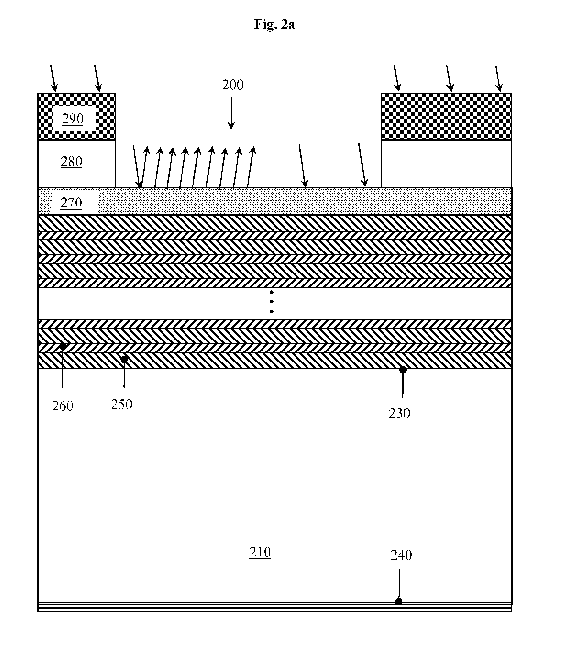
[0178]This part of the specification is organized as follows: It begins with the introduction of some technical terms and of some problems with respect to photolithographic masks and then describes the apparatus used to correct these problems (“photolithographic masks and laser system”). In the second part entitled “registration problems” the inventive method is then applied in order to primarily correct registration errors of a photolithographic mask. A third part entitled “CDU problems” discusses the application of the inventive principle in order to primarily correct critical dimension uniformity (CDU) problems. Further, in the fourth part entitled “overlay problems” the inventive method is used in order to minimize overlay problems between different photolithographic masks in a stack of masks. Finally, the theoretical and / or mathematical background of the inventive method necessary for the discussion of the various examples in this section is presented in an own section entitled...


PUM

PropertyMeasurementUnit
wavelengthaaaaaaaaaa
wavelength rangeaaaaaaaaaa
rotation angleaaaaaaaaaa

Abstract

A method for correcting a plurality of errors of a photolithographic mask, comprising optimizing first parameters of a imaging transformation of the photolithographic mask and second parameters of a laser beam locally directed onto the photolithographic mask, and correcting the plurality of errors by applying an imaging transformation using optimized first parameters and locally directing the laser beam onto the photolithographic mask using optimized second parameters, wherein the first and the second parameters are simultaneously optimized in a joint optimization process.

Description

CROSS-REFERENCE TO RELATED APPLICATIONS[0001]Under 37 C.F.R. §119 this application claims the benefit of priority from U.S. provisional application Ser. No. 61 / 363,352, filed Jul. 12, 2010, the contents of which are incorporated by reference in their entirety.FIELD OF THE INVENTION[0002]The present invention relates to the field of correcting errors of a photolithographic mask.BACKGROUND OF THE INVENTION[0003]As a result of the constantly increasing integration density in the semiconductor industry, photolithographic masks have to project smaller and smaller structures onto a photosensitive layer, e.g., a photoresist on wafers. In order to fulfil this demand, the exposure wavelength of photolithographic masks has been shifted from the near ultraviolet across the mean ultraviolet into the far ultraviolet region of the electromagnetic spectrum. Presently, a wavelength of 193 nm is typically used for the exposure of the photoresist on wafers. As a consequence, the manufacturing of phot...

Claims


Application Information

Patent Timeline
Patent Type & Authority Applications(United States)
IPC IPC(8): G03F1/00B29C35/08
CPCG03F1/72G03F7/70625G03F7/70466G03F1/84H01L21/0274H01L21/0275
Inventor DMITRIEV, VLADIMIR
Owner CARL ZEISS SMS GMBH
Why Eureka
Try Eureka