

Reduced-step CMOS processes for low-cost radio frequency identification devices
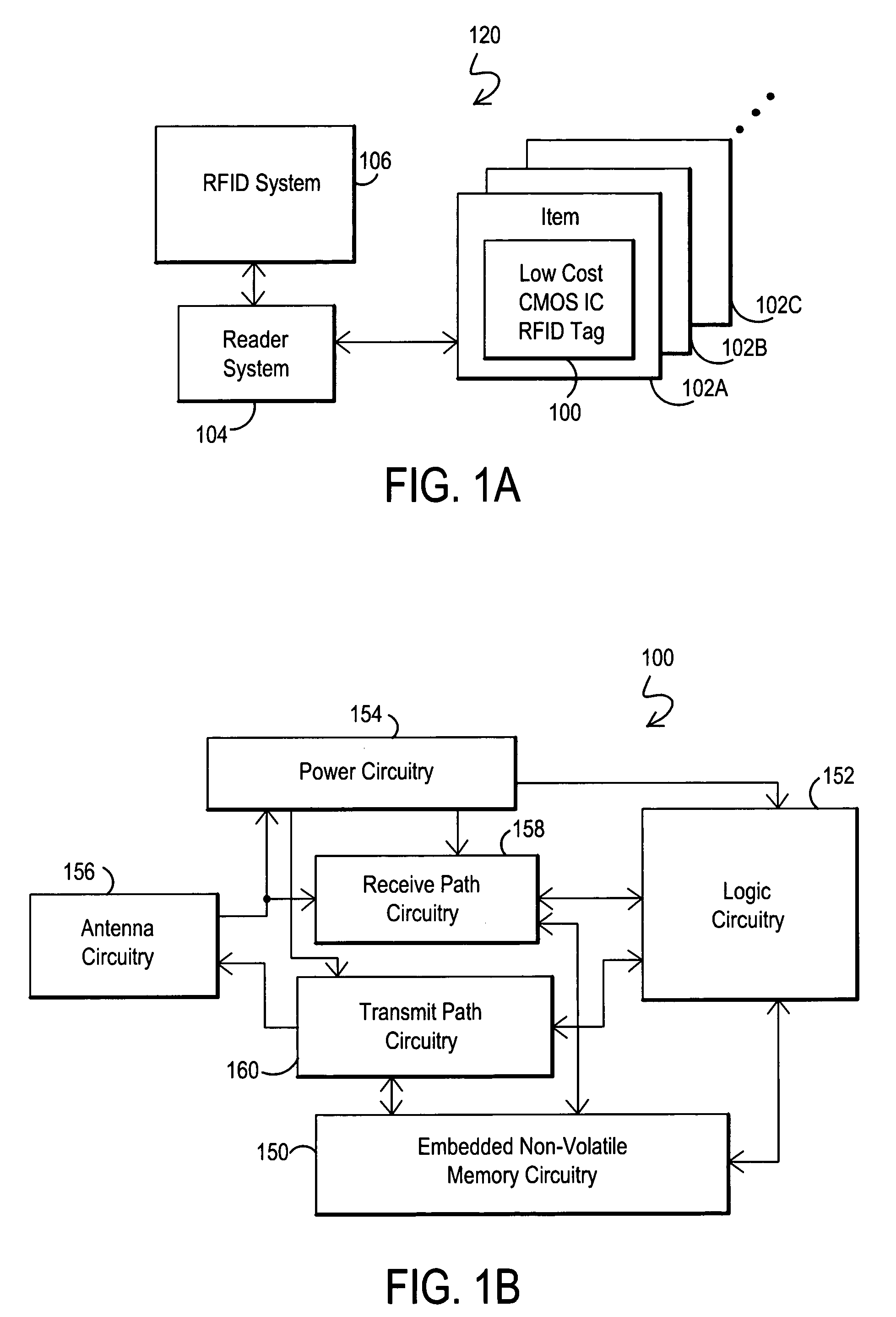
a radio frequency identification and process technology, applied in the field of radio frequency identification (rfid) systems, can solve the problems that the fabrication of rfid devices may cost five cents or less, and achieve the effect of reducing the step cmos
- Summary
- Abstract
- Description
- Claims
- Application Information
AI Technical Summary
Benefits of technology
Problems solved by technology
Method used
Image

Examples
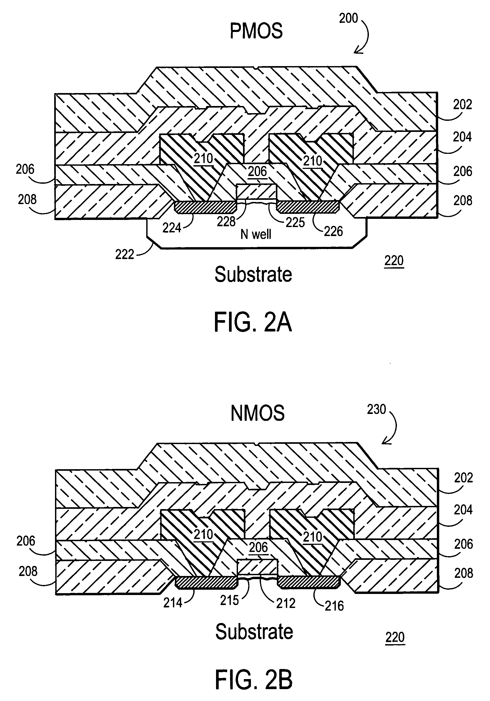
embodiment 200
[0037]FIG. 2A is a process layer diagram for a PMOS transistor made using a low-cost, reduced step CMOS process according to the present invention. In the embodiment 200 depicted, a substrate 220 can be a P-type substrate. An N-type well 222 is formed within the substrate 220. Regions 208 are barrier layers and can be formed, for example, as silicon dioxide layers. These barrier layers 208 form protective field oxide regions between adjacent active devices. Gate oxide 225, which lies above the N-type channel for the PMOS transistor and underlies the gate 228, can also be formed as a silicon dioxide layer. Regions 224 and 226 are the source and drain for the PMOS transistor and are formed by doping these active regions to be P-type. Region 228 is the gate for the PMOS transistor and can be formed, for example, by forming a polysilicon layer. Regions 206 represent a non-conductive layer that provides a polysilicon-to-metal dielectric layer. Regions 204 represent an inter-metal dielect...
embodiment 230
[0038]FIG. 2B is a process layer diagram for an NMOS transistor made using a low-cost, reduced step CMOS process according to the present invention. In the embodiment 230 depicted, a substrate 220 can be a P-type substrate. Regions 208 are barrier layers and can be formed, for example, as silicon dioxide layers. As above, these barrier layers 208 form protective field oxide regions between adjacent active devices. Gate oxide 215, which lies above the P-type channel for the NMOS transistor and underlies the gate 212, can also be formed as a silicon dioxide layer. Regions 214 and 216 are the source and drain for the NMOS transistor and are formed by doping these active regions to be N-type. Region 212 is the gate for the NMOS transistor and can be formed, for example, by forming a polysilicon layer. Regions 206 represent a non-conductive layer that provides a polysilicon-to-metal dielectric layer. Regions 204 represent an inter-metal dielectric layer that provides a non-conductive lay...
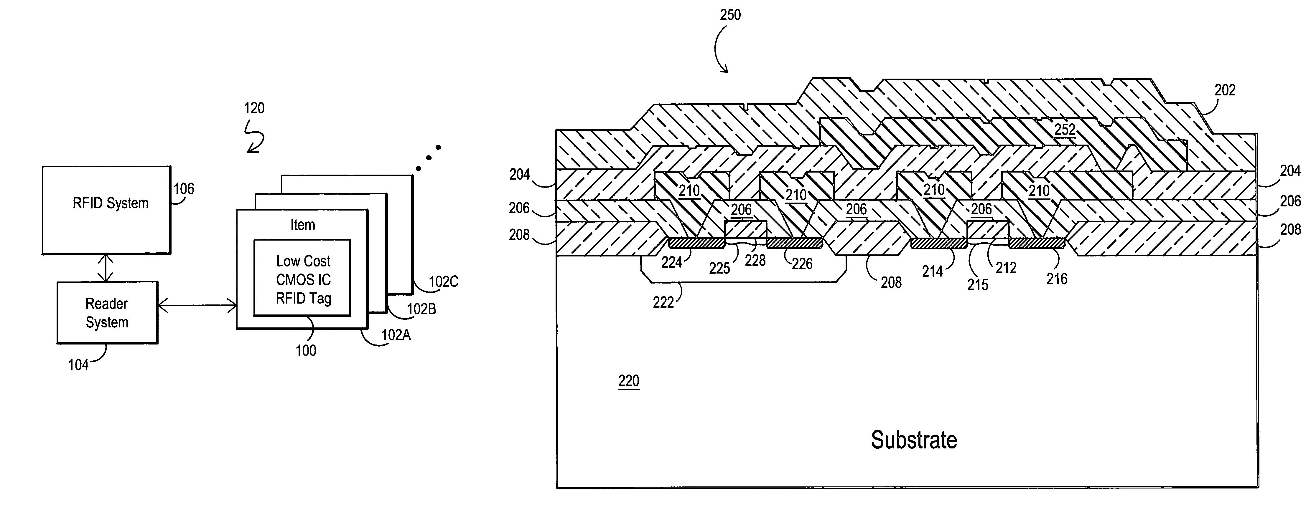
embodiment 250
[0039]FIG. 2C is a process layer diagram for a PMOS transistor and an NMOS transistor made using a low-cost, reduced step CMOS process according to the present invention. In the embodiment 250 depicted, a substrate 220 can be a P-type substrate. An N-type well 222 is formed within the substrate 220. Regions 208 are barrier layers and can be formed, for example, as silicon dioxide layers. These barrier layers 208 form protective field oxide regions between adjacent active devices. The gate oxide 225 and the gate oxide 215 can also be formed as a silicon dioxide layer. As above, regions 224 and 226 are the source and drain for the PMOS transistor and are formed by doping these active regions to be P-type. Region 228 is the gate for the PMOS transistor and can be formed, for example, by forming a polysilicon layer. As above, regions 214 and 216 are the source and drain for the NMOS transistor and are formed by doping these active regions to be N-type. Region 212 is the gate for the NMO...
PUM
 Abstract
Description
Claims
Application Information