High bandwidth cache-to-processing unit communication in a multiple processor/cache system

a cache-to-processing unit and high-bandwidth technology, applied in the field of semiconductor devices, can solve the problems of limiting the practical use of stacked semiconductors, the size of the semiconductor and their functions, and the inability to efficiently address the data communication bandwidth and the size or package footprint in multiple processing core systems

Inactive Publication Date: 2010-08-17
NORTH STAR INNOVATIONS
View PDF17 Cites 217 Cited by
  • Summary
  • Abstract
  • Description
  • Claims
  • Application Information

AI Technical Summary

Problems solved by technology

The size of the semiconductors and their functions continue to limit the practical use of stacked semiconductors, as well as the ability to efficiently make electrical connections to multiple semiconductors in close proximity.
Efficiently addressing both the data communication bandwidth and the size or package footprint issues in multiple processing core systems remains problematic.

Method used


Image

  • High bandwidth cache-to-processing unit communication in a multiple processor/cache system
  • High bandwidth cache-to-processing unit communication in a multiple processor/cache system
  • High bandwidth cache-to-processing unit communication in a multiple processor/cache system

Examples


Embodiment Construction

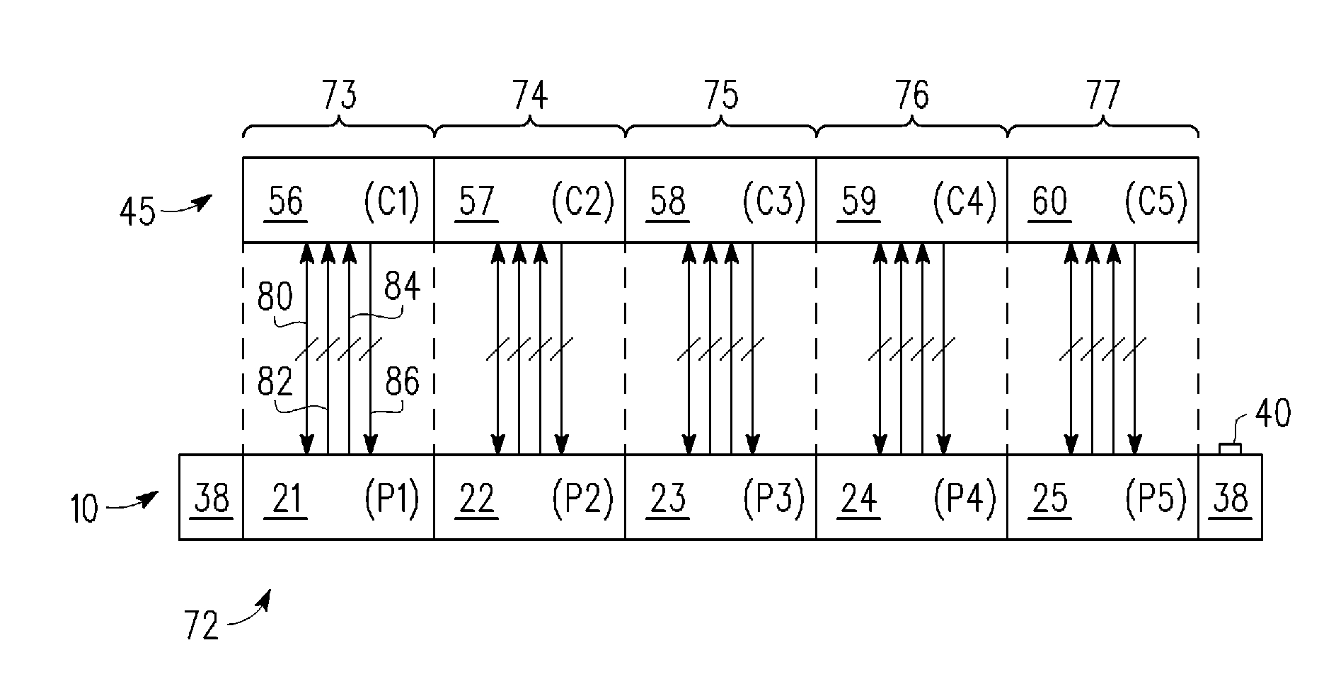
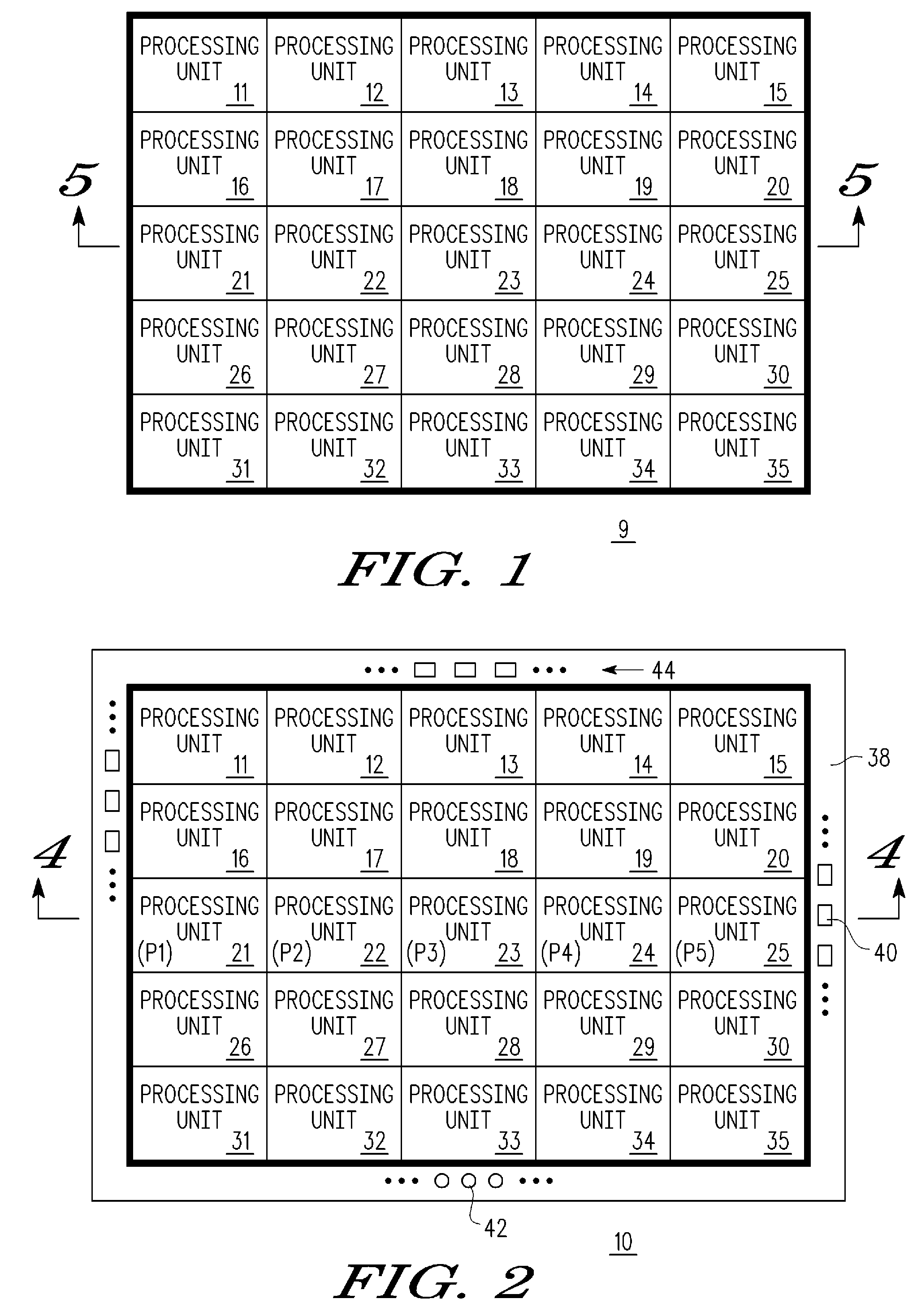
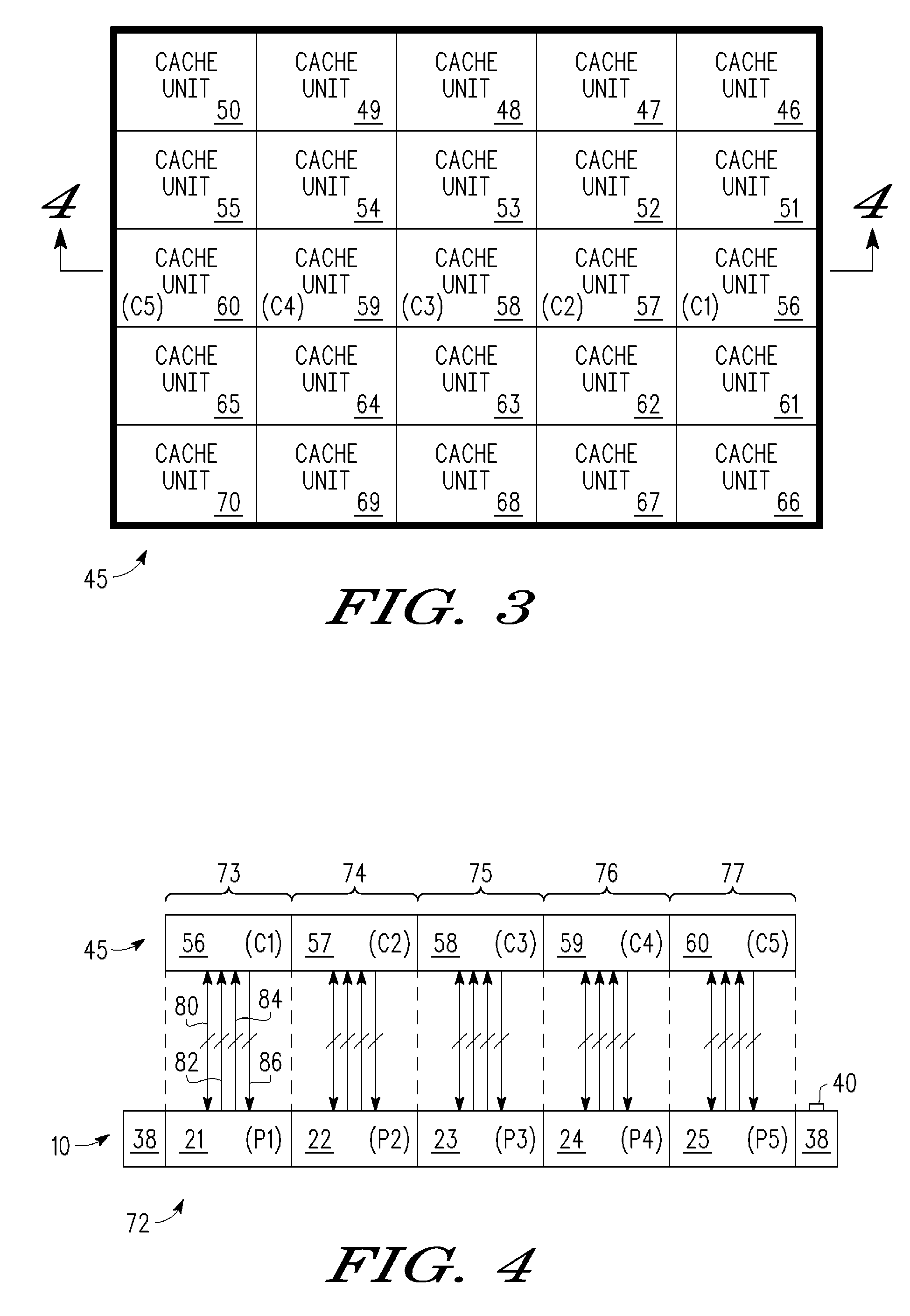
[0013]Illustrated in FIG. 1 is a major surface of a processor die 9 having a plurality of individual and separate processing units 11-35 provided in an array having rows and columns. In other forms the processing units 11-35 may be placed in an array of geometric configurations other than rows and columns of processing units. Each of the processing units 11-35 is any type of a variety of data processors. For example, each of the processing units 11-35 may be a central processing unit (CPUs), a digital signal processor, a graphics-specific processor, a microcontroller unit (MCU), a communications processor or any other type of processing unit. Further, the processing units 11-35 may be the same type of processing unit or may vary between types of processing unit across the processor die 9. In the illustrated form there are five rows with each processing unit row having five columns. It should be understood that the illustrated embodiment is exemplary only and any number of X rows and...


PUM


Abstract

A processor / cache assembly has a processor die coupled to a cache die. The processor die has a plurality of processor units arranged in an array. There is a plurality of processor sets of contact pads on the processor units, one processor set for each processor unit. Similarly, the cache die has a plurality of cache units arranged in an array. There is a plurality of cache sets of contact pads on the cache die, one cache set for each cache unit. Each cache set is in contact with one corresponding processor set.

Description

BACKGROUND[0001]1. Field[0002]This disclosure relates generally to semiconductors, and more specifically, to processing operating speeds that exist in semiconductor packages having multiple die.[0003]2. Related Art[0004]It is well known to stack two or more semiconductor packages on top of each other to reduce footprint area. Others have also proposed stacking two or more semiconductor die on top of each other. Various solutions have been proposed for addressing problems associated with additional heat that is generated when two separate semiconductors are placed in close proximity with each other. The size of the semiconductors and their functions continue to limit the practical use of stacked semiconductors, as well as the ability to efficiently make electrical connections to multiple semiconductors in close proximity.[0005]Commercial data processing systems typically utilize multiple cores or processing units. For example, it is common in the desktop processing environment for du...

Claims


Application Information

Patent Timeline
Patent Type & Authority Patents(United States)
IPC IPC(8): H01L23/34
CPCH01L23/49827H01L23/50H01L25/0657H01L25/50H01L23/147H01L2224/16235H01L23/4985H01L24/05H01L24/16H01L2224/32145H01L2924/30105H01L2924/30107H01L2225/06517H01L2225/06575H01L2225/06589H01L2225/06513H01L2225/06541H01L2224/05553H01L2224/0401H01L23/49816
Inventor PELLEY, PERRY H.MCSHANE, MICHAEL B.
Owner NORTH STAR INNOVATIONS
Why Eureka
Try Eureka