Light emitting device

a technology light sources, which is applied in the direction of semiconductor devices, electric lighting sources, electric light sources, etc., can solve the problems of overheating and damage of light emitting diodes, and achieve the effect of efficient output of optimal pulse power, and suppressing the amount of generated hea

Inactive Publication Date: 2010-08-17
HAYASHI KAGAKU INDS
View PDF11 Cites 4 Cited by
  • Summary
  • Abstract
  • Description
  • Claims
  • Application Information

AI Technical Summary

Benefits of technology

[0008]An object of the present invention is to provide a light emitting device capable of suppressing the amount of heat generated by a light emitting diode and preventing the light emitting diode from being overheated without reducing the amount of light even when the light emitting diode is a high-power light emitting diode.
[0011]The light emitting device defined in claim 1 converts a DC power into a pulse power by means of the switching regulator 13, lowers the voltage of this pulse power by means of the output control portion 14, adjusts the pulse width of this pulse power by means of the pulse width adjusting oscillation means 16, further limits the current of this pulse power by means of the limiting resistor 17 and then outputs this pulse power to the light emitting diodes 11. Due to this, since an optimum pulse power can be efficiently outputted to a light emitting diode 11 even if it is a high-power light emitting diode 11, it is possible to suppress the amount of heat generated without reducing the amount of light of the light emitting diode 11.
[0015]The light emitting device defined in claim 3 can suppress the amount of generated heat without reducing the amount of light of a light emitting diode 11 even when it is a high-power light emitting diode 11.
[0016]According to the present invention, since a light emitting device is configured so that a switching regulator converts a DC power into a pulse power, an output control portion lowers the voltage of this pulse power, a pulse width adjusting oscillation means adjusts the pulse width of this pulse power, and further a limiting resistor limits and outputs the current of this pulse power to a light emitting diode, it is possible to efficiently output the optimum pulse power for a light emitting diode even when it is a high-power light emitting diode. As a result, since it is possible to suppress the amount of generated heat without reducing the amount of light of the light emitting diode, it is possible to prevent the light emitting diode from being overheated.
[0017]And when one end of a first resistor the other end of which is connected to a compared voltage input of a voltage comparator of a switching regulator is grounded through a waveform shaping capacitor, one end of a second resistor the other end of which is connected to the compared voltage input of the above-mentioned voltage comparator is grounded, the first resistor has a resistance value of 3.0 kΩ to 9.0 kΩ, the second resistor has a resistance value of 1.0 kΩ to 2.0 kΩ, the ratio in resistance value of the first resistor to the second resistor is 1.5 to 9.0, and the limiting resistor has a resistance value of 1.0 Ω to 100.0 Ω, it is possible to set the voltage and current of a pulse power to be outputted to a light emitting diode at the respective optimum values for making the light emitting diode emit light. As a result, it is possible to efficiently output the optimum pulse power to the light emitting diode.
[0018]Even by using as a light emitting diode a high-power light emitting diode having a forward current of 100 mA to 1000 mA, a pulse forward current of 200 mA to 2000 mA, a allowable reverse current of 50 mA to 250 mA, a power dissipation of 1.0 to 8.0 W, an operating temperature of −30 to 85° C., a storage temperature of −40 to 100° C., and a dice temperature of 80 to 160° C., it is also possible to suppress the amount of generated heat without reducing the amount of light of a light emitting diode. As a result, it is possible to prevent the light emitting diode from being overheated.

Problems solved by technology

In a light emitting device disclosed in the above-mentioned conventional Patent Document 1, however, in case of using a high-power light emitting diode, there has been the possibility that the light emitting diode is overheated and damaged due to the increase in amount of heat generated by the light emitting diode when the electric current to flow through the light emitting diode is increased in order to increase the amount of light of it.

Method used


Image

  • Light emitting device
  • Light emitting device
  • Light emitting device

Examples


first embodiment

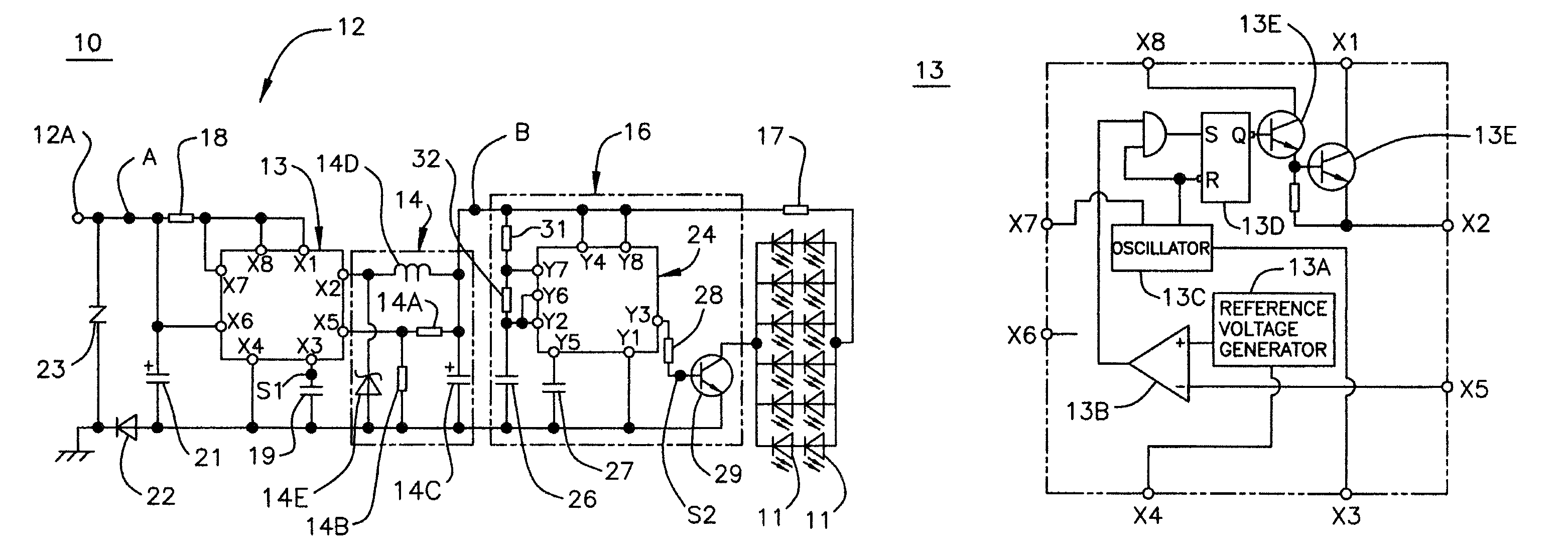
[0036]As shown in FIG. 1, a light emitting device 10 comprises twenty light emitting diodes 11 and a lighting circuit 12 for lighting these light emitting diodes 11. The twenty light emitting diodes 11 are configured so as to connect in parallel six sets of light emitting diodes 11, said sets each having two light emitting diodes connected in series. A high-power light emitting diode is used as each of these light emitting diodes 11. Concretely, there is used a light emitting diode having a forward current of 100 mA to 1000 mA, preferably 400 mA to 700 mA, a pulse forward current of 200 mA to 2000 mA, preferably 350 mA to 1000 mA, a allowable reverse current of 50 mA to 250 mA, preferably 80 mA to 150 mA, a power dissipation of 1.0 to 8.0 W, preferably 1.5 to 5 W, an operating temperature of −30 to 85° C., preferably −30 to 80° C., a storage temperature of −40 to 100° C., preferably 0 to 80° C., and a dice temperature of 80 to 160° C., preferably 80 to 120° C. (for example, LED of a...

example 1

[0047]As shown in FIG. 1, a light emitting device 10 was configured by connecting twelve light emitting diodes 11 to a lighting circuit 12. The twenty light emitting diodes 11 were connected so as to connect in parallel six sets of light emitting diodes, said sets each having two light emitting diodes connected in series. The resistance value of the first resistor 14a of the output control portion 14 was set at 7.5 kΩ, the resistance value of the second resistor 14b was set at 1.3 kΩ, and the resistance value of the limiting resistor 17 was set at 2.2 Ω. The second heat-radiating member 42 to have the light emitting diode 11 mounted on it and the base member 43 to have the second heat-radiating member 42 mounted on it used ABS resin rather than a high thermal-conductivity resin (FIG. 5). This light emitting device 10 was determined as example 1.

example 2

[0048]A light emitting device was configured in the same way as example 1 except lighting by means of a lighting circuit ten light emitting diodes connected so as to connect in parallel five sets of light emitting diodes, said sets each having two light emitting diodes connected in series. This light emitting device was determined as example 2.


PUM


Abstract

An object of the invention is to suppress the amount of heat generated by a light emitting diode and prevent the light emitting diode from being overheated without reducing the amount of emitted light even when the light emitting diode is a high-power light emitting diode. A light emitting device is configured so that one or more light emitting diodes (11) are lighted by a lighting circuit (12). A DC power is converted into a pulse power by a switching regulator (13) of this lighting circuit (12) and the voltage of a pulse power converted by this switching regulator is lowered by an output control portion (14). The pulse width of a pulse power lowered in voltage by this output control portion is adjusted by a pulse width adjusting oscillation means (16), and the current of a pulse power adjusted in pulse width by this pulse width adjusting oscillation means is limited by a limiting resistor (17). The light emitting device is configured so that a pulse power limited in current by this limiting resistor is outputted to a light emitting diode.

Description

BACKGROUND OF THE INVENTION[0001]1. Field of the Invention[0002]The present invention relates to a light emitting device for lighting a light emitting diode (LED) by means of a lighting circuit.[0003]2. Description of the Invention[0004]Up to now, as a device of this kind, there has been disclosed a light emitting device for simultaneously lighting light emitting diodes of a light emitting unit by making a lighting circuit receive a DC power from a DC power source, said light emitting unit being formed by arranging a plurality of light emitting diodes and connecting these light emitting diodes with each other (see Patent Document 1 for example). This light emitting device is configured so that a DC power is inputted into a switching regulator of the lighting circuit from a DC power source and this switching regulator performs a switching operation according to the magnitude of electric current flowing through the light emitting unit. And it is configured so that a pulse current obta...

Claims


Application Information

Patent Timeline
Patent Type & Authority Patents(United States)
IPC IPC(8): H05B37/02H01L33/00
CPCH05B33/0818H05B45/3725
Inventor MISHIMAGI, KAZUHARU
Owner HAYASHI KAGAKU INDS
Why Eureka
Try Eureka