

Alignment apparatus, exposure apparatus, and device manufacturing method
a technology of exposure apparatus and alignment apparatus, which is applied in the direction of multi-dynamo-electric motor speed regulation, control mechanism, magnetic circuit, etc., can solve the problems of affecting the image quality of the projection optical system and and affecting the measurement accuracy of the leaser interferometer. , to achieve the effect of reducing the influence, reducing the influence of ambient temperature change, and high accuracy of alignmen
- Summary
- Abstract
- Description
- Claims
- Application Information
AI Technical Summary
Benefits of technology
Problems solved by technology
Method used
Image

Examples
first embodiment
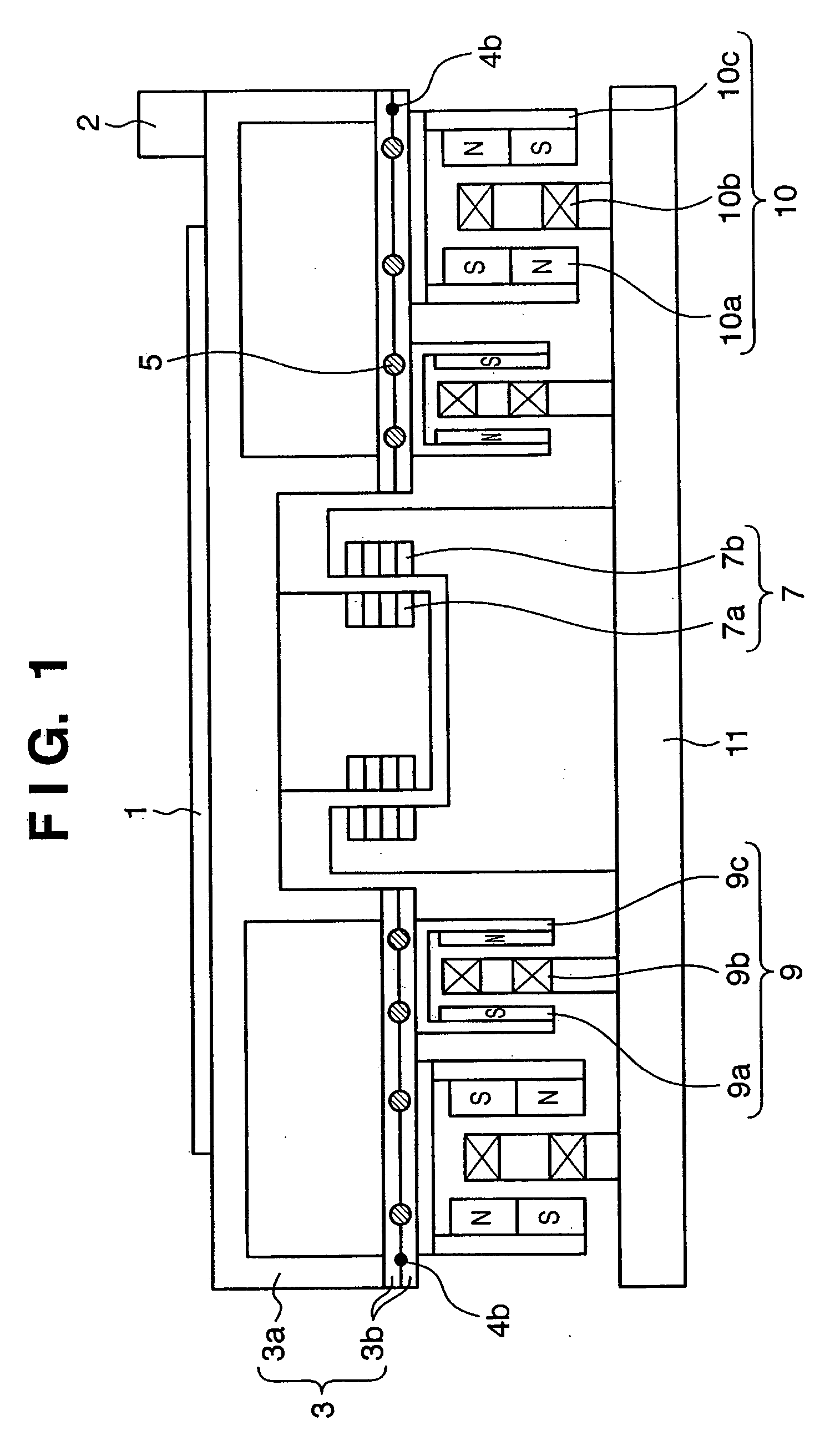
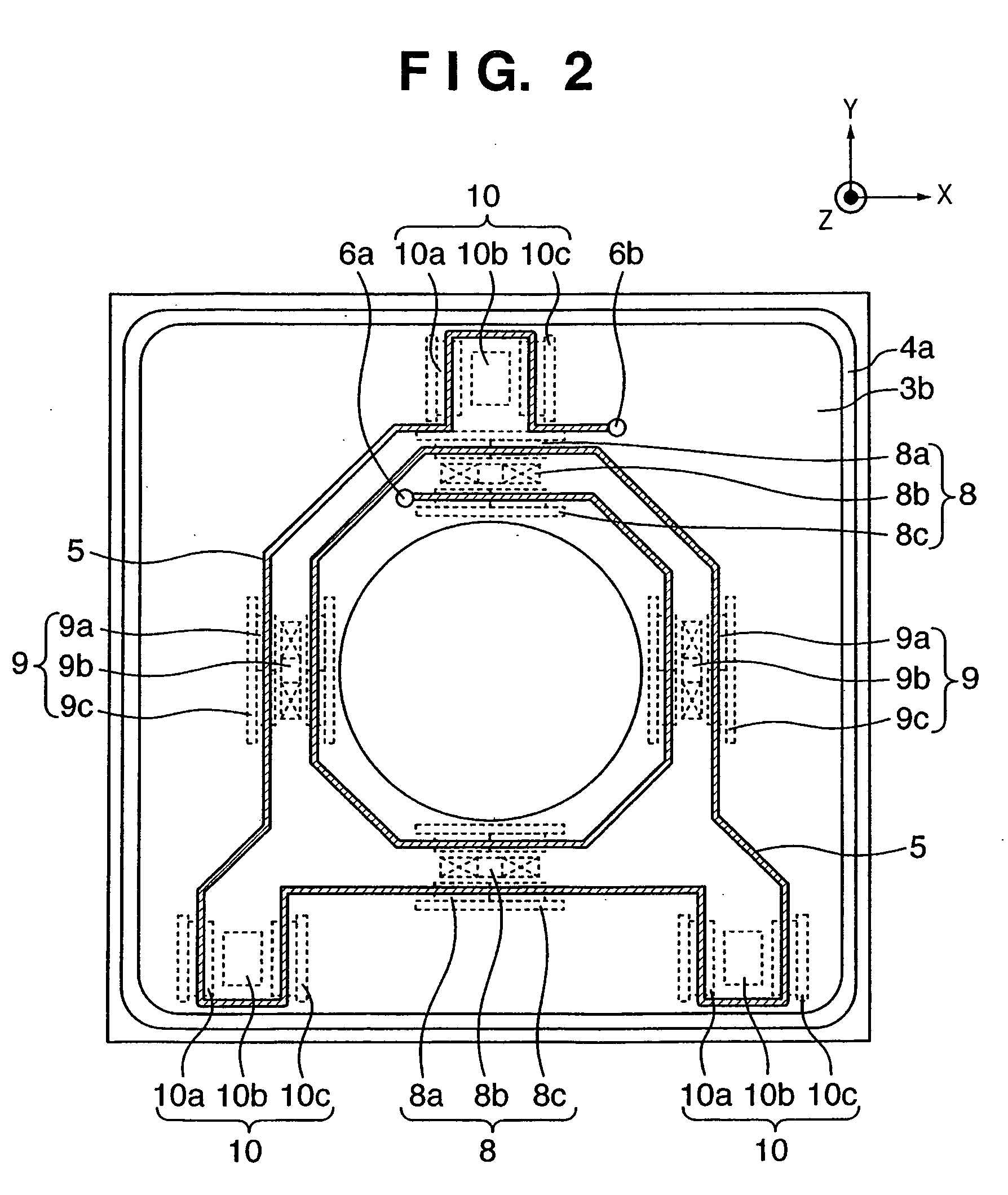
[0050]FIG. 1 is a schematic sectional view showing a fine-movement stage which forms an alignment apparatus according to the first embodiment of the present invention, and its peripheral portions, and FIG. 2 is a perspective view seen from the top of a top panel which forms the fine-movement stage according to the first embodiment of the present invention, and its peripheral portions.
[0051] The fine-movement stage includes a chuck 1, bar-mirrors 2, a top panel (movable stage main body) 3, electromagnetic couplings 7, X-direction fine-movement linear motors 8 which have a self-weight compensating mechanism and transfer support rod (neither is shown) and serve to finely adjust the position of the top panel 3, Y-direction fine-movement linear motors 9, Z-direction fine-movement linear motors 10, and the like. These components are disposed on an X-Y slider 11 to form the fine-movement stage.
[0052] The top panel 3 comprises a first structure 3a (upper plate) formed of a hollow box-like...
second embodiment
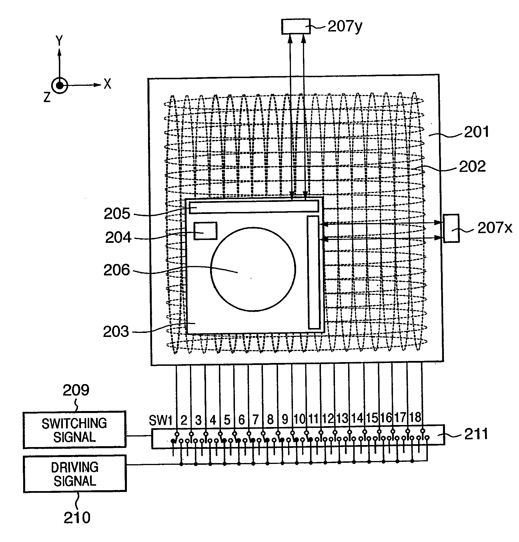
[0061]FIGS. 3A and 3B are plan and side views, respectively, showing the arrangement of a guideless 6-axis flat stage serving as an alignment apparatus according to the second embodiment of the present invention.
[0062] Referring to FIGS. 3A and 3B, reference numeral 201 denotes a base structure; 202, a driving coil group (stators); 203, a movable stage main body (movable element) serving as a flat stage; 204, a sensor; 205, bar-mirrors; 206, a chuck; 207×, an X-direction laser interferometer; 207y, a Y-direction laser interferometer; 208, permanent magnets; 209, a switching signal; 210, a driving signal; and 211, a selector switch, respectively.
[0063] In the flat stage shown in FIGS. 3A and 3B, the driving coil group 202 is arranged in a matrix in the base structure 201. Similarly, the permanent magnets 208 are arranged in a matrix on the lower portion of the movable stage main body 203. The plurality of permanent magnets 208 are magnetized in a predetermined direction and periodi...
third embodiment
[0081]FIG. 7 is a perspective view showing the second structure of a top plate which forms an alignment apparatus according to the third embodiment of the present invention, and its peripheral portions, FIG. 8 is a plan view of the second structure, FIG. 9 is a sectional view taken along the line b-b of FIG. 8, and FIG. 10 is an enlarged view of a portion B of FIG. 9. The arrangement of other peripheral portions is the same as that in the second embodiment, and a detailed description thereof will be omitted.
[0082] As shown in FIG. 7, grooves 35a and 35b which form a helically extending inner flow passage 35, and an inlet 36a and outlet 36b to supply a refrigerant to the inner flow passage 35 are formed in a second structure 33b which forms the bottom plate of the top panel. One inlet 36a and one outlet 36b suffice, but pluralities of inlets 36a and outlets 36b also will do. The grooves which form the inner flow passage 35 are preferably formed such that the line resistance acting w...
PUM
| Property | Measurement | Unit |
|---|---|---|
| temperature | aaaaa | aaaaa |
| degrees of freedom | aaaaa | aaaaa |
| wavelength | aaaaa | aaaaa |
Abstract
Description
Claims
Application Information