Semiconductor device, ink cartridge, and electronic device
a semiconductor and ink technology, applied in the direction of printing, other printing devices, etc., can solve the problems of waste of remaining ink, complex sensor structure, and errors in the amount of ink consumption,
- Summary
- Abstract
- Description
- Claims
- Application Information
AI Technical Summary
Benefits of technology
Problems solved by technology
Method used
Image
Examples
first embodiment
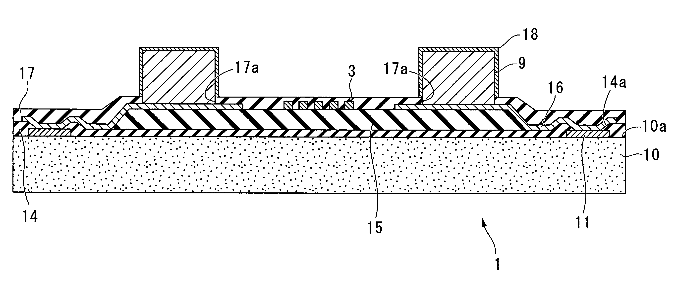
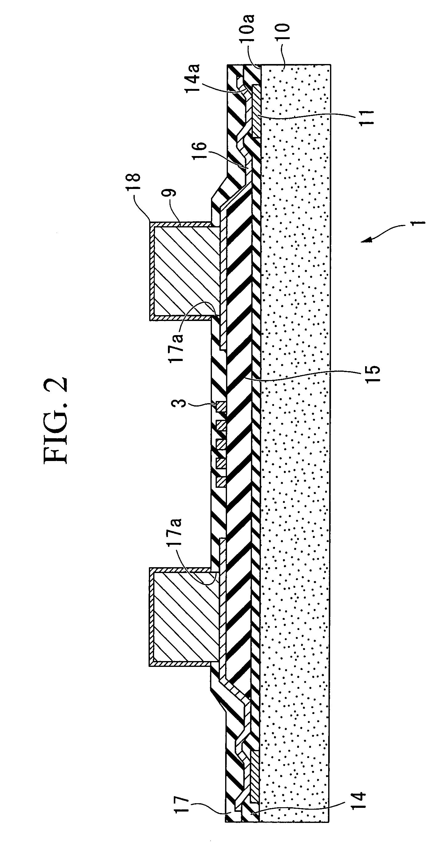
[0095]FIG. 2 is a cross-sectional view of a semiconductor device of the invention.
[0096]FIG. 3 is an exterior view of a first embodiment of a semiconductor device of the invention.
[0097]In these diagrams, reference numeral 1 represents a semiconductor device having a wafer level chip scale package (W-CSP) structure.
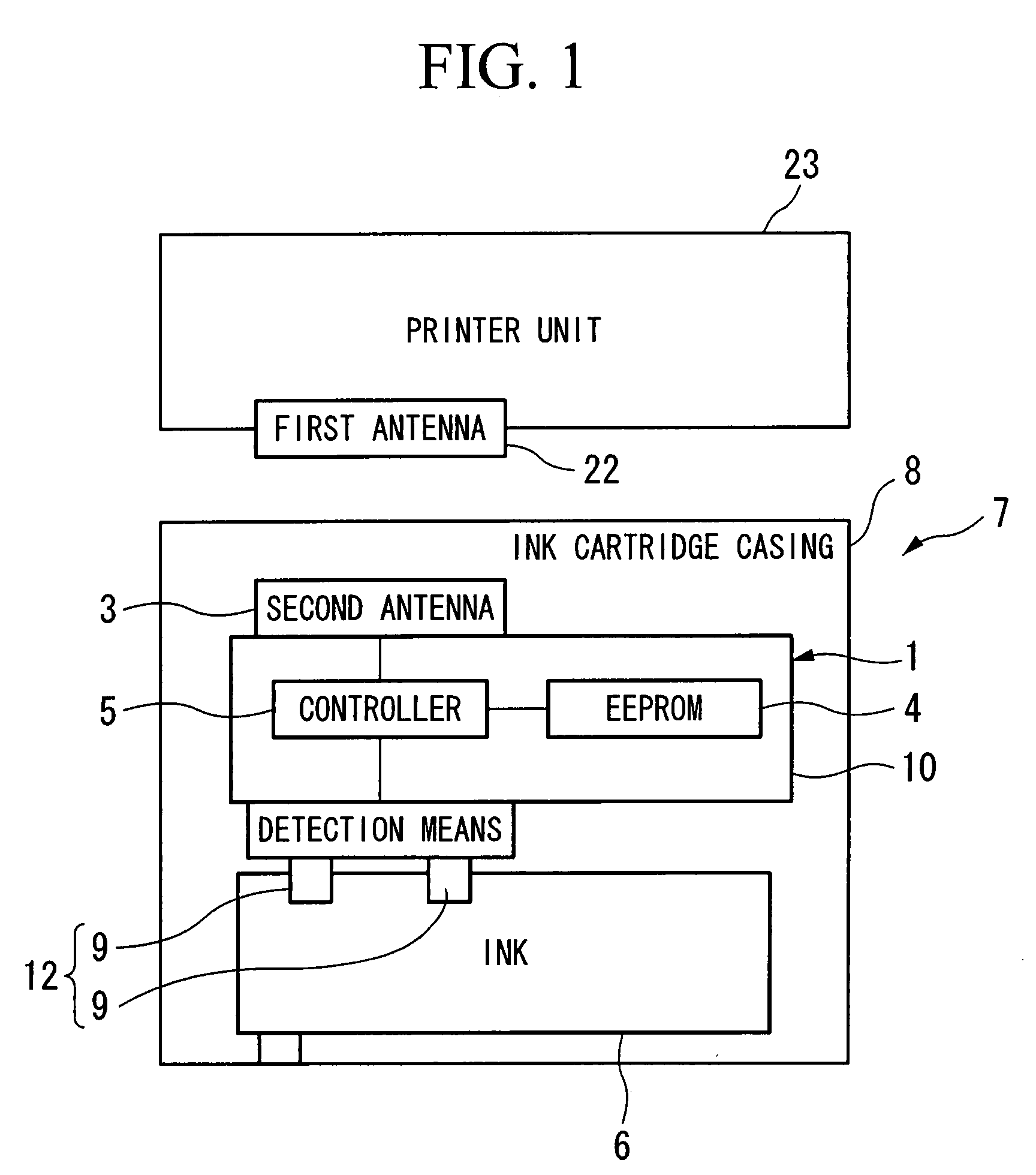
[0098]The semiconductor device 1 includes liquid contact electrodes 9 (detection electrodes), a second antenna 3, an EEPROM 4 (storage circuit), and a controller 5 (control circuit), which are provided on a rectangular semiconductor substrate 10.
[0099]The liquid contact electrodes 9 detect a remaining amount of ink.
[0100]The second antenna 3 transmits and receives information to / from a first antenna 22 of the printer unit 23. The EEPROM 4 stores ink information.
[0101]The controller 5 controls the liquid contact electrodes 9, the second antenna 3, and the EEPROM 4.
[0102]The semiconductor substrate 10 is made from silicon.
[0103]An integrated circuit (not shown) includes the...
second embodiment
[0182]A second embodiment will be described with reference to FIG. 7.
[0183]Reference numeral 41 represents a semiconductor device of the invention.
[0184]This embodiment differs from the first embodiment in that parts of the relocation interconnections 16 exposed through the openings 17a in the protective layer 17 are used as liquid contact electrodes 12 (detection electrodes).
[0185]This embodiment detects ink information when the relocation interconnections 16 are wetted by ink infiltrating into the openings 17a.
[0186]To achieve this, an Au-plated film (not shown) having excellent chemical resistance is provided above the relocation interconnections 16 exposed through the openings 17a in the same manner as described above.
[0187]This Au-plated film prevents ink from infiltrating the semiconductor device 41 from the openings 17a.
[0188]As a result, it is possible to prevent the ink from affecting the active elements (integrated circuit) on the active element formation face 10a of the...
PUM
 Abstract
Description
Claims
Application Information


