Top emitting, electroluminescent component with frequency conversion centres

a technology of electroluminescent components and top emitting, which is applied in the direction of discharge tube/lamp details, discharge tube luminescnet screens, organic semiconductor devices, etc., can solve the problems of low efficiency, low coupling efficiency, and low coupling efficiency, so as to improve coupling efficiency

Active Publication Date: 2010-08-24
NOVALED GMBH
View PDF47 Cites 2 Cited by
  • Summary
  • Abstract
  • Description
  • Claims
  • Application Information

AI Technical Summary

Benefits of technology

[0008]The invention is based on the object of improving the coupling-out efficiency for light in a top emitting, electroluminescent component of the generic type. This object is achieved in a surprisingly simple manner in terms of a device just by means of a component having the features of claim 1. In this case, the top emitting electroluminescent component according to the invention, which may be formed in particular as an organic light-emitting diode device, comprises a substrate, a first electrode nearest to the substrate, a second, transparent electrode located at a distance from the substrate, and at least one organic layer arranged between the two electrodes, at least one of the organic layers being a light-emitting layer. The component is distinguished according to the invention by virtue of the fact that a coupling-out layer is arranged on that side of the second electrode which is remote from the at least one organic layer, said coupling-out layer comprising frequency conversion centres which partly absorb the light emitted in the at least one organic layer and emit it again with an altered frequency.
[0009]The invention's configuration of the top emitting, electroluminescent component enables the coupling-out efficiency thereof to be increased by more than 100%, depending on the specific embodiment, in comparison with the conventional configuration of such a component without a coupling-out layer. Furthermore, the coupling-out layer can also perform even further functions besides the function specified.
[0010]The invention is based on the idea, with the provision of a coupling-out layer on that side of the second electrode which is remote from the organic layer or layers, of influencing the propagation of the optical modes within the organic layers and the transparent electrode such that the coupling-out efficiency is increased. For this purpose, conversion centres are provided in the coupling-out layer, which conversion centres partly absorb the light emitted by the at least one organic layer and emit it again with an altered frequency. In this way, directional light penetrating into the coupling-out layer is emitted again in non-directional fashion, so that a part of the light which would be captured by means of total reflection without the influence of the frequency conversion centres within the coupling-out layer can indeed leave the coupling-out layer.

Problems solved by technology

However, they have some disadvantages, such as the great angular dependence of contrast and colours, slow response times in the event of picture and contrast change, and a low efficiency caused by a multiplicity of filters and polarizers, so that comparatively high energies have to be used for obtaining the required luminous intensity.

Method used


Image

  • Top emitting, electroluminescent component with frequency conversion centres
  • Top emitting, electroluminescent component with frequency conversion centres
  • Top emitting, electroluminescent component with frequency conversion centres

Examples


Embodiment Construction

[0057]The invention is explained below by the description of a plurality of embodiments with reference to the accompanying Fig., in which

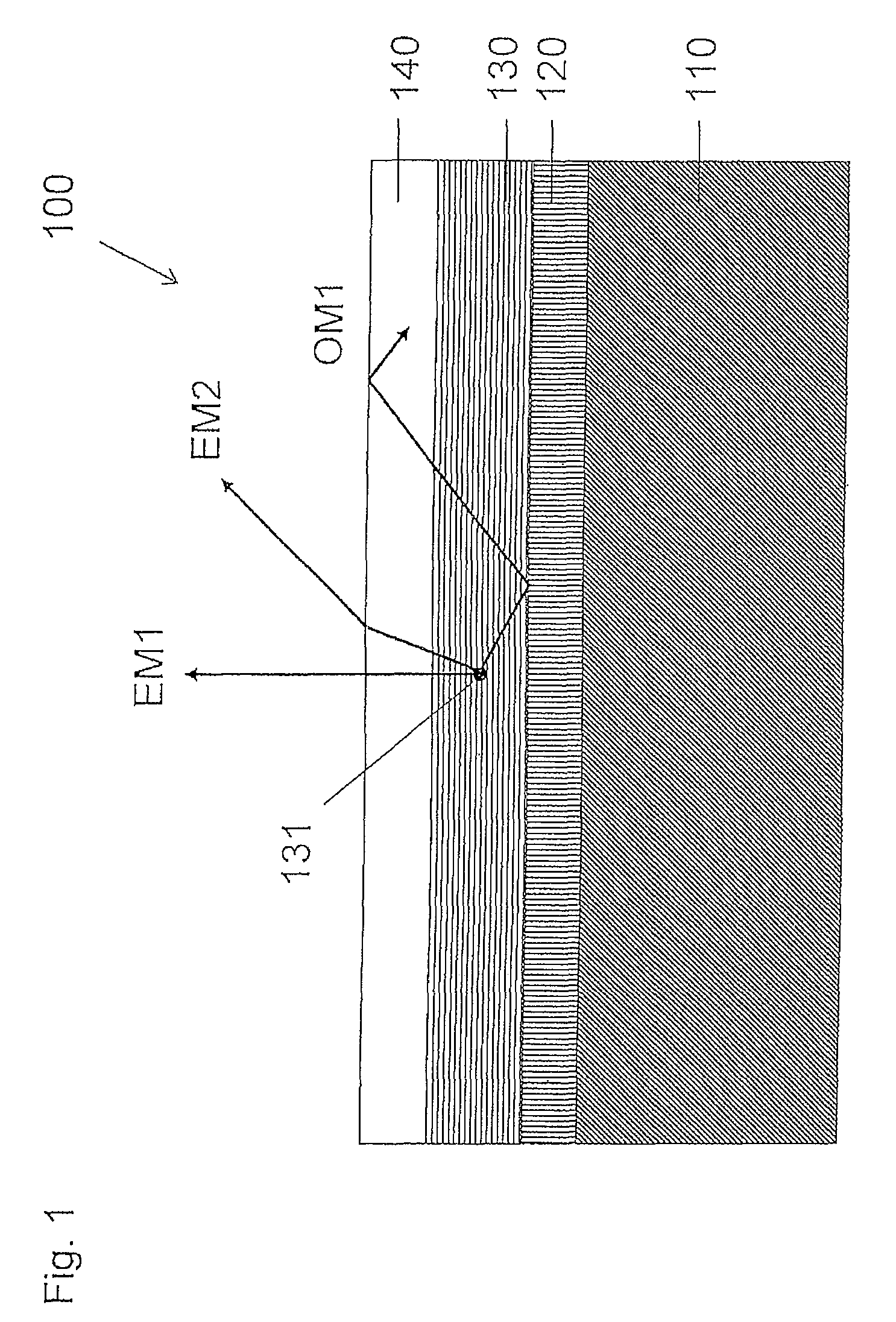
[0058]FIG. 1 shows a conventional top emitting OLED in a schematic illustration,

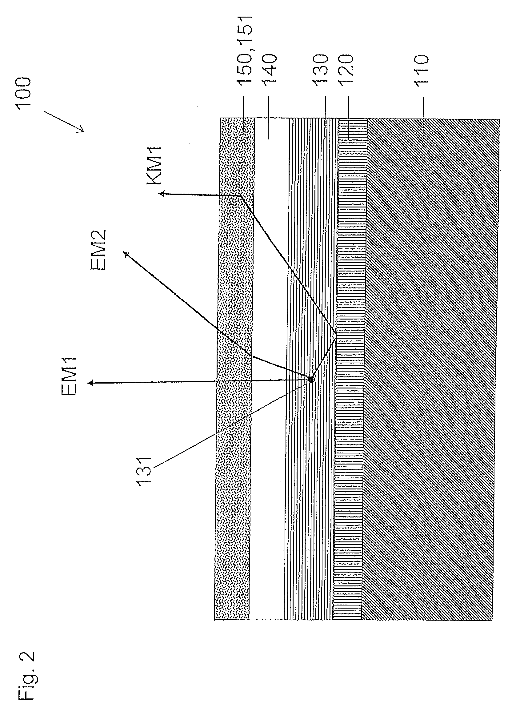
[0059]FIG. 2 shows a top emitting OLED designed according to the invention in accordance with a first embodiment in a schematic illustration.

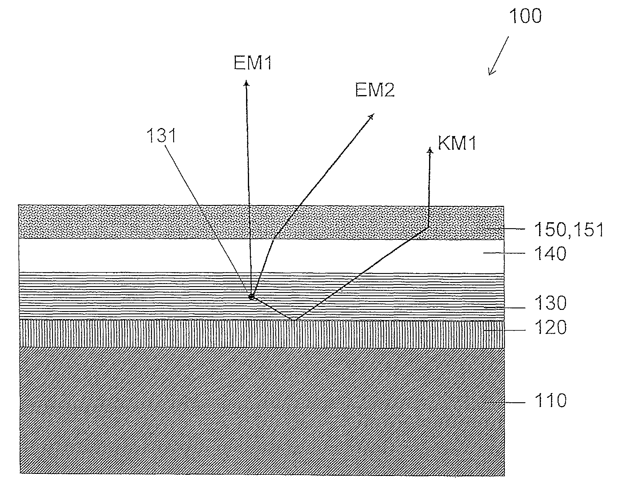
[0060]FIG. 1 shows a schematic sketch of the construction of a conventional electroluminescent, top emitting component 100. In the example specified, the electrode 120 nearest to the substrate 110, which electrode is designated hereinafter as first electrode, is embodied as a reflective metal layer. A plurality of organic layers, specified as organic layer structure 130 in the Fig., are applied to the first electrode. Said layer structure comprises at least one organic electroluminescent layer. The layer structure 130 is adjoined by a second electrode 140 composed of a transparent material, for example a conductive oxide.

[0061]When...


PUM


Abstract

In order, in the case of an OLED, to improve the coupling-out efficiency, a top emitting electroluminescent component (100) is proposed, comprising a substrate (110), a first electrode (120) closest to the substrate, a transparent electrode (140) located at a distance from the substrate, and at least one light-emitting organic layer (130) arranged between the two electrodes. The component according to the invention is distinguished by the fact that a coupling-out layer (150) is arranged on that side of the second electrode which is remote from the at least one organic layer, said coupling-out layer comprising conversion centres (151) which partly absorb the light emitted by the at least one organic layer and emit it again with an altered frequency. In this way, directional light penetrating into the coupling-out layer is emitted again in non-directional fashion, so that a part of the light which would be captured by means of total reflection without the influence of the frequency conversion centres within the coupling-out layer can indeed leave the coupling-out layer.

Description

[0001]The invention relates to a top emitting, electroluminescent component and to a method for producing it.BACKGROUND OF THE INVENTION[0002]In recent years a high demand has developed for ever smaller, space-saving, light and cost-effective display modules and displays for fast and adequate visualization of data. In the field of flat screens for notebooks, mobile telephones and digital cameras, LCDs (liquid crystal displays) are still predominant at the present time. However, they have some disadvantages, such as the great angular dependence of contrast and colours, slow response times in the event of picture and contrast change, and a low efficiency caused by a multiplicity of filters and polarizers, so that comparatively high energies have to be used for obtaining the required luminous intensity. In this respect, there is a high demand for small high-resolution and power-saving screens with improved presentation properties. Displays based on organic light-emitting diodes (OLEDs)...

Claims


Application Information

Patent Timeline
Patent Type & Authority Patents(United States)
IPC IPC(8): H05B33/04
CPCH01L51/5262H01L51/5036H01L2251/5315H10K50/125H10K50/85H10K2102/3026H10K50/852H10K50/858
Inventor BIRNSTOCK, JANVEHSE, MARTINLEO, KARL
Owner NOVALED GMBH
Why Eureka
Try Eureka