Mass production testing of USB flash cards with various flash memory cells

a technology of flash memory cells and usb flash cards, applied in the field of mass production testing of usb electronic data flash cards, can solve the problems of unauthorized access to confidential information, significant amount of time, and conventional testing methods that cannot keep up with the increasing manufacturing volume, so as to facilitate high-volume formatting/testing of usb devices, facilitate efficient and high-volume testing/formatting of usb devices, and eliminate time-consuming and unnecessary registration processes

Inactive Publication Date: 2010-08-31
SUPER TALENT TECH CORP
View PDF43 Cites 45 Cited by
  • Summary
  • Abstract
  • Description
  • Claims
  • Application Information

AI Technical Summary

Benefits of technology

[0013]The present invention is also directed to a high volume testing / formatting process for Universal Serial Bus-based (USB-based) electronic data flash cards (USB devices) that meets the increasing demand for USB electronic data flash cards (USB devices). In particular, a system and method is provided for high volume formatting / testing of USB devices in which a test host is simultaneously coupled to the multiple USB devices (e.g., using a multi-port card reader or a probe fixture), a controller endpoint value is read from each of the USB devices and verified with a known good value, and then formatting is performed on each of the USB devices in a “pipelined” manner by writing predetermined data into each USB device. The USB devices are then tested by reading out and testing the predetermined data. In one embodiment, the test host implements a special USB driver that blocks standard USB registration procedures upon detecting the plurality of USB devices. By bypassing conventional USB registration procedures and verifying the controller endpoint values before testing / formatting, the present invention facilitates the efficient and high volume testing / formatting of USB devices by eliminating the time consuming and unnecessary registration process. In addition, by writing data into the USB devices in a “pipelined” manner, the present invention facilitates high volume formatting / testing of USB devices that greatly reduces production time.
[0014]In accordance with an aspect of the present invention, each USB device is modified to minimize controller ROM size by storing selected control code data, boot code data, device information and configuration information on the flash memory device. Because much of this code and information is required and accessed during the conventional USB registration process (i.e., because the conventional USB registration process presumes this code and information is available in controller ROM), bypassing the conventional USB registration process provides a further function of avoiding system failure or long delays as the host system waits for this code and information when an un-formatted USB device (with blank flash memory device) is coupled to the test host.
[0015]In accordance with another aspect of the present invention, the purpose of the testing / formatting process includes checking that all chips are correctly soldered, that current consumption levels meet specifications, and that each component device (e.g., the controller and flash memory devices) is compatible with the testing / formatting program being implemented by the test host system. The formatting process serves to load all entry point values needed for correct controller operation, erase the flash memory and build up redundant bad_block_list files for future bad block management, and to provide low level formatting that that facilitates OS recognition.

Problems solved by technology

However, confidential data files and documents are exposed to the danger that the passwords, encryption codes, safety seals and impressions may be broken (deciphered), thereby resulting in unauthorized access to the confidential information.
With increasing production volume, a problem faced by the manufacturer is how to efficiently and reliably test the USB flash cards before shipping to the end users.
A problem with such conventional testing methods utilizing PC is that normal PC Windows™ (or MAC™) operating systems only support a few USB devices at a time, and a significant amount of time is required to manually plug in each USB flash card, for the operating system to detect and test the USB flash cards, and then to manually unplug each USB flash card.
As such, conventional testing methods cannot keep up with the increasing manufacturing volume.

Method used


Image

  • Mass production testing of USB flash cards with various flash memory cells
  • Mass production testing of USB flash cards with various flash memory cells
  • Mass production testing of USB flash cards with various flash memory cells

Examples


Embodiment Construction

[0048]The present invention relates to an improvement in methods for producing electronic data flash cards. Although the present invention is described below with specific reference to USB electronic data flash cards, the present novel aspects of the present invention can be used in the manufacture of a wide range of flash card types, including but not limited to PCI Express, Secure Digital (SD), Memory Stick (MS), Compact Flash (CF), IDE and SATA flash memory cards.

[0049]FIGS. 21A-21G show one embodiment of extended USB connectors and sockets having metal contact pins on both top and bottom surfaces of the pin substrates.

[0050]FIGS. 22A-22I show a second embodiment of extended USB connectors and sockets having metal contact pins on just one of the surfaces of the pin substrates.

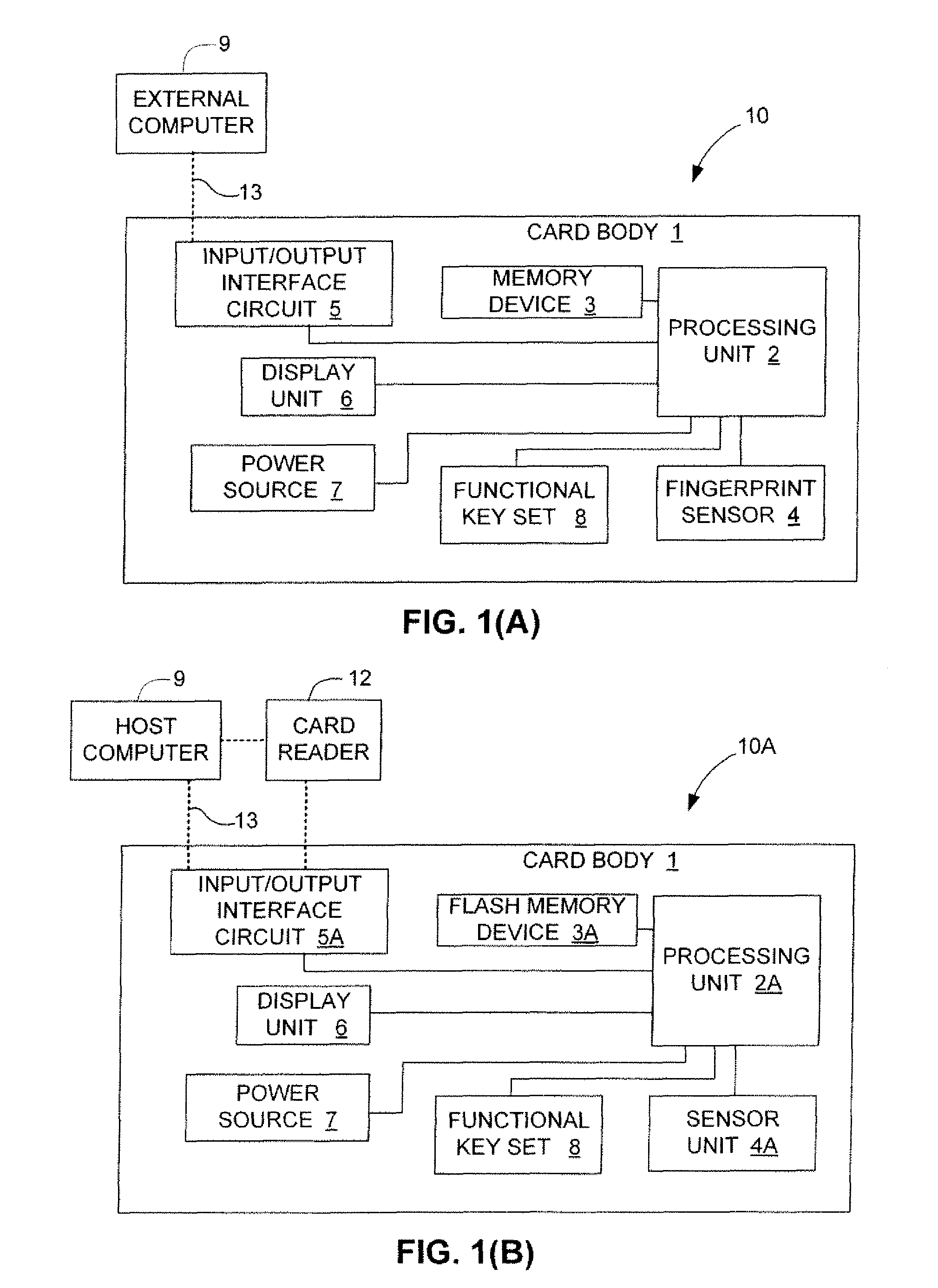
[0051]Referring to FIG. 1(A), according to an embodiment of the present invention, an electronic data flash card 10 is adapted to be accessed by an external (host) computer 9 either via an interface bus 13 o...


PUM


Abstract

A high volume testing / formatting process is provided for Universal Serial Bus-based (USB-based) electronic data flash cards (USB devices) that meets the increasing demand for USB electronic data flash cards (USB devices). A test host is simultaneously coupled to the multiple USB devices (e.g., using a multi-port card reader or a probe fixture), a controller endpoint value is read from each of the USB devices and verified with a known good value, and then testing / formatting is performed on each of the USB devices by writing predetermined data into each USB device in a pipelined manner, then reading out and testing the predetermined data. In one embodiment, the test host implements a special USB driver that blocks standard USB registration procedures upon detecting the plurality of USB devices. Control and / or boot code data are written onto the flash memory device (i.e., instead of being provided on a controller ROM).

Description

RELATED APPLICATIONS[0001]This application is a continuation-in-part (CIP) of U.S. patent application Ser. No. 11 / 626,347, filed Jan. 23, 2007, now U.S. Pat. No. 7,702,984, entitled “High Volume Testing for USB Electronic Data Flash Cards”, and “Flash Memory Controller For Electronic Data Flash Card”, U.S. application Ser. No. 11 / 466,759, filed on Aug. 23, 2006 now U.S. Pat. No. 7,702,831, which is a CIP of “System and Method for Controlling Flash Memory”, U.S. application Ser. No. 10 / 789,333, filed on Feb. 26, 2004, now U.S. Pat. No. 7,318,117.[0002]This application is also a CIP of U.S. patent application Ser. No. 11 / 737,336, filed Apr. 19, 2007, entitled “Cell-Downgrading and Reference-Voltage Adjustment for a Multi-bit-cell Flash Memory”, now U.S. Pat. No. 7,333,364.[0003]This application is also a CIP of U.S. patent application Ser. No. 11 / 864,696, filed Sep. 28, 2007, entitled “Backward Compatible Extended USB Plug And Receptacle With Dual Personality”, which is a CIP of U.S. ...

Claims


Application Information

Patent Timeline
Patent Type & Authority Patents(United States)
IPC IPC(8): G11C29/00G01R31/28G11C16/04
CPCG06F11/2221
Inventor CHOW, DAVID Q.MA, ABRAHAM C.LEE, EDWARD W.SHEN, MING-SHIANG
Owner SUPER TALENT TECH CORP
Why Eureka
Try Eureka