Current switch circuit and D/A converter, semiconductor integrated circuit, and communication device using the same

a technology of switching circuit and d/a converter, which is applied in the direction of code conversion, pulse technique, instruments, etc., can solve the problems of power reduction and low power voltage, and achieve the effects of reducing the area of a semiconductor chip, wide output voltage range, and increasing power consumption

Active Publication Date: 2010-09-14
PANASONIC CORP
View PDF14 Cites 13 Cited by
  • Summary
  • Abstract
  • Description
  • Claims
  • Application Information

AI Technical Summary

Benefits of technology

[0047]As described above, according to the present invention, a wide output voltage range was realized without causing deterioration in properties of the current switch circuit by determining the threshold voltage of the first and second transistors included in the differential switch at a high level, it is possible to reduce an increase in the area of a semiconductor chip and an increase in power consumption and to maintain the output voltage range within a constant predetermined range regardless of the production process variations.

Problems solved by technology

Although current steering D / A converters are essential which enable a high speed operation in LSIs for video and communication, the power voltage is low due to power reduction.

Method used


Image

  • Current switch circuit and D/A converter, semiconductor integrated circuit, and communication device using the same
  • Current switch circuit and D/A converter, semiconductor integrated circuit, and communication device using the same
  • Current switch circuit and D/A converter, semiconductor integrated circuit, and communication device using the same

Examples


first embodiment

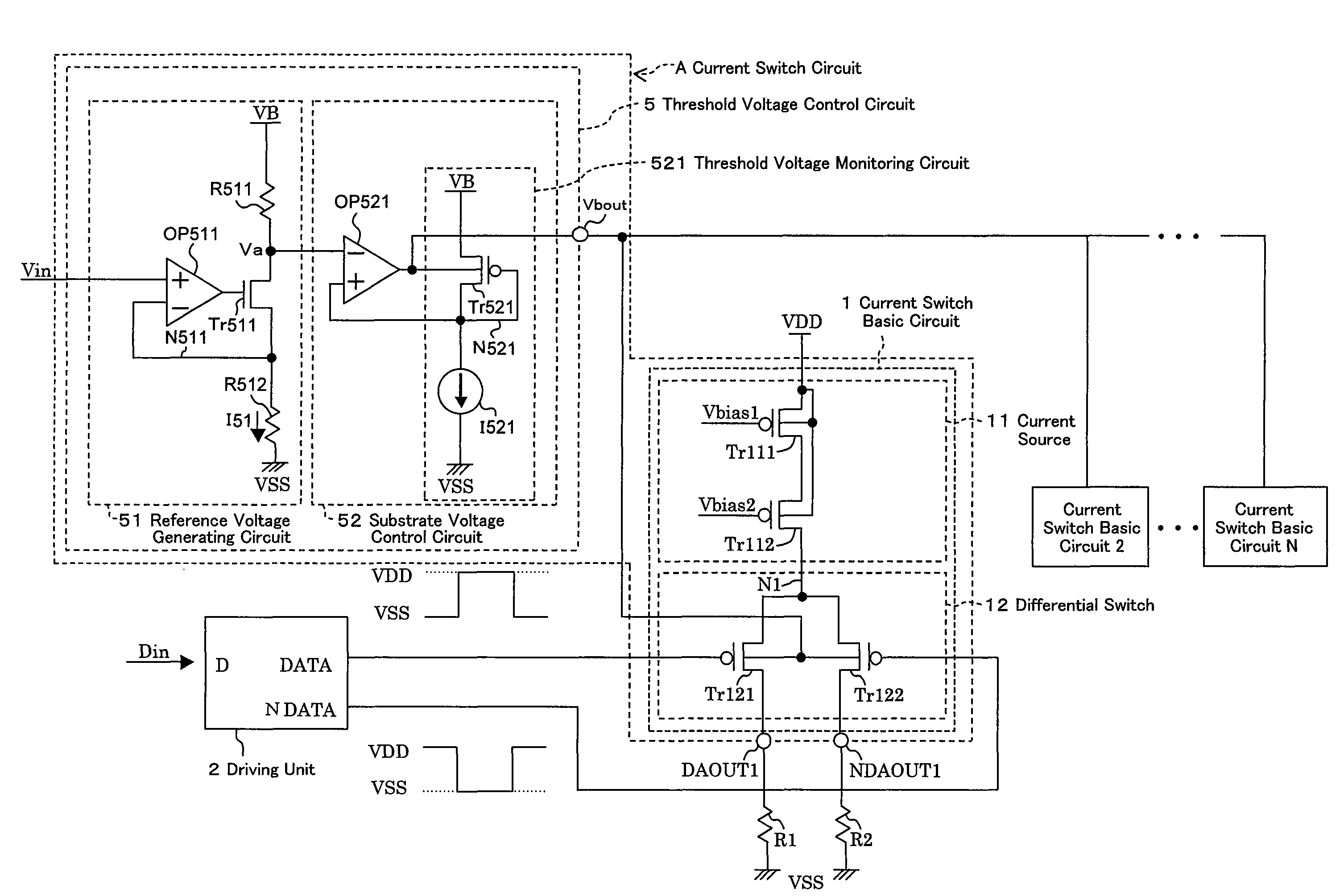
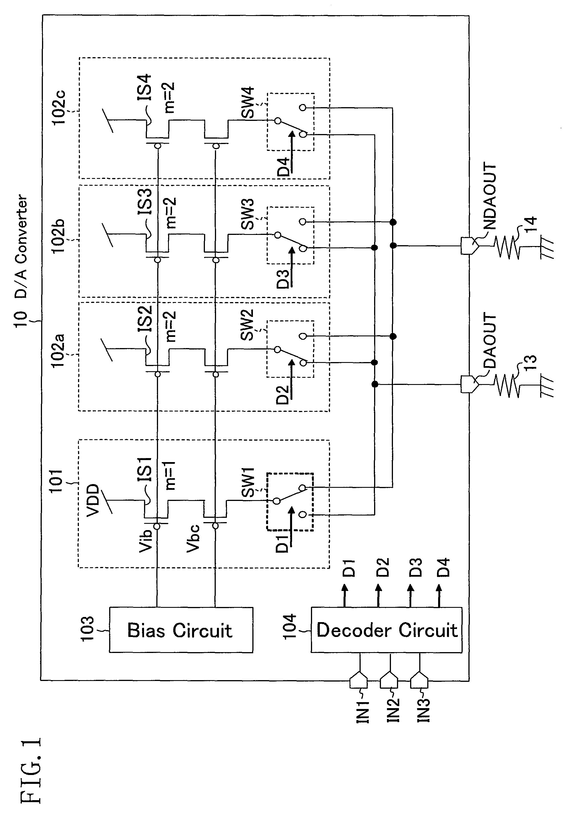
[0076]FIG. 1 shows the overall schematic structure of a D / A converter including a current switch circuit of this embodiment.

[0077]FIG. 1 shows a current steering D / A converter 10 which converts a 3-bit digital signal to an analog signal. The D / A converter 10 includes four current sources IS1 to IS4 each consisting of transistors connected in cascode, and the current value of the current sources is determined by bias voltages Vib and Vbc applied from a bias circuit 103 to respective gate terminals.

[0078]Respective output terminals of the current sources IS1 to IS4 are connected to differential switches SW1 to SW4 to form a current switch basic circuit101. The current switch basic circuit 101 is a current switch basic circuit (a lower current switch) for LSB which outputs an LSB current, and the current switch basic circuits 102a to 102c are three current switch basic circuits (upper current switches) for MSB which output MSB currents. The upper current switch basic circuits 102a to 1...

second embodiment

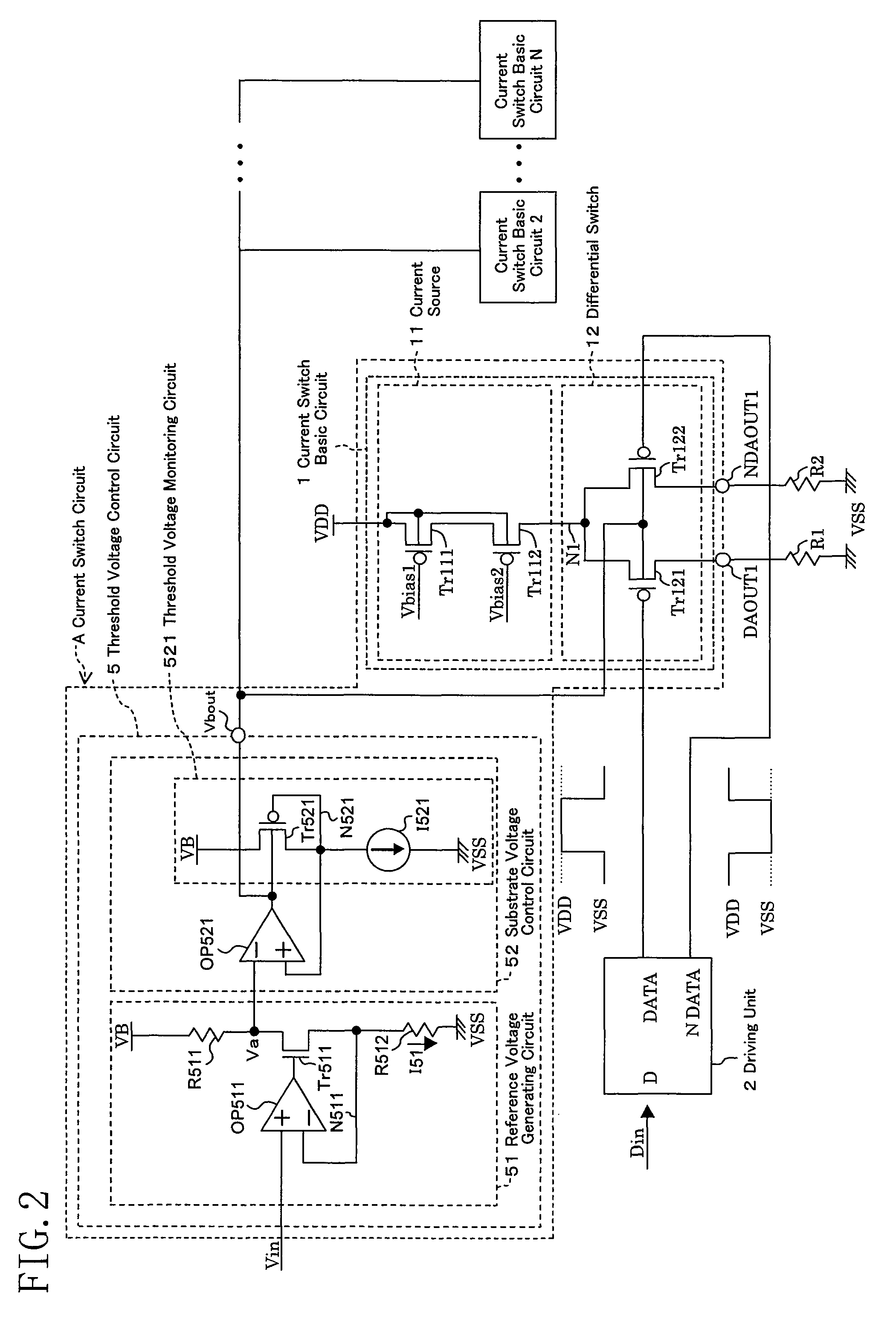
[0110]FIG. 3 is a block diagram of the current switch basic circuit 1, the driving unit 2, and the output load resistors R1 and R2 showing the second embodiment of the present invention. Different from the first embodiment, the current switch circuit A does not include a threshold voltage control circuit inside.

[0111]The current switch basic circuit 1 includes the current source 11 and the differential switch 12. The current source 11 for an operation at a low power voltage includes the low voltage withstanding P channel type MOS transistors Tr111 and Tr112 each having a thin gate insulating film. The transistor Tr111 has the source terminal connected to the first power potential VDD, the drain terminal connected to the source terminal of the transistor Tr112, and the gate terminal to which stabilized voltage Vbias1 is applied. The other transistor Tr112 has the drain terminal connected to the node N1 and the gate terminal to which stabilized voltage Vbias2 is applied. Each of the t...

third embodiment

[0122]FIG. 4 shows the structure of the current switch basic circuit 1, the driving unit 2, and the output load resistors R1 and R2 in the current switch circuit A showing the third embodiment of the present invention. Different from the first embodiment, the current switch circuit A does not include a threshold voltage control circuit inside.

[0123]In FIG. 4, the current switch basic circuit 1 includes the current source 11 and the differential switch 12. The current source 11 for an operation at a low power voltage includes the low voltage withstanding P channel type MOS transistors Tr111 and Tr112 each having a thin gate insulating film. The transistor Tr111 has the source terminal connected to the first power potential VDD, the drain terminal connected to the source terminal of the transistor Tr112, and the gate terminal to which stabilized voltage Vbias1 is applied. The other transistor Tr112 has the drain terminal connected to the node N1 and the gate terminal to which stabiliz...


PUM


Abstract

In a current switch circuit A used for a current steering D / A converter, a current switch basic circuit 1 includes first and second transistors Tr121 and Tr122 included in a differential switch 12. A threshold voltage control circuit 5 has an output terminal Vbout controlling the substrate voltage to be outputted to the substrate terminal of each of the two transistors Tr121 and Tr122 included in the differential switch 12 for controlling the threshold voltage of the two transistors of the differential switch. Accordingly, the present invention improves the decrease in the dynamic range of the current switch basic circuit 1 dependent on the threshold of each of the two transistors in the differential switch 12 and realizes a wider output voltage range without causing deterioration in properties even in a case that the power voltage is reduced in the current switch basic circuit 1.

Description

RELATED APPLICATIONS[0001]This application is the U.S. National Phase under 35 U.S.C. §371 of International Application No. PCT / JP2007 / 070649, filed on Oct. 23, 2007, which in turn claims the benefit of Japanese Application No. 2007-002608, filed on Jan. 10, 2007, the disclosures of which Applications are incorporated by reference herein.TECHNICAL FIELD[0002]The present invention relates to a current switch circuit, and particularly relates to a technique for a D / A converter (DAC) for communication that ameliorates the problem of a decrease in the dynamic range under low power voltage to realize a wider output voltage range.BACKGROUND ART[0003]In recent years, to take advantage of low costs of CMOS, SOCs (System On Chip) were increasingly produced which mixed digital and analog circuits on one chip. In contrast, various information appliances were introduced to the market in recent years, and semiconductor integrated circuit devices, particularly LSIs, used for such appliances are d...

Claims


Application Information

Patent Timeline
Patent Type & Authority Patents(United States)
IPC IPC(8): H03M1/66
CPCH03K17/302H03K17/687H03K2217/0018H03M1/742
Inventor OGAWA, TOMOHIROIKOMA, HEIJI
Owner PANASONIC CORP
Why Eureka
Try Eureka