Electrical device utilizing charge recycling within a cell

a cell and charge recycling technology, applied in the direction of basic electric elements, electromagnetic wave modulation, instruments, etc., can solve the problems of impairing the light modulating capabilities of individual pixels or cells, the difficulty of producing desired gel relief profiles with good precision, and the power consumption becomes very important, so as to improve the performance and properties of the enhanced electrodes. , the effect of increasing the power consumption of the device and improving the performance and properties

Inactive Publication Date: 2009-07-28
NOKIA CORP
View PDF10 Cites 80 Cited by
  • Summary
  • Abstract
  • Description
  • Claims
  • Application Information

AI Technical Summary

Benefits of technology

[0008]However, the Applicant has noticed, that the enhancement electrode performance and properties especially regarding the power consumption may be further significantly improved. Thus, the main purpose of the present invention is to provide a novel and simple scheme for powering the enhancement electrodes, thus making the use of enhancement electrodes possible without significantly increasing the power consumption of the device. Together with the teachings given in PCT / FI02 / 00512, the enhancement electrode driving system according to the current invention helps to manufacture light modulators that have good optical properties combined with low power consumption. Such optical modulators find many applications and can be used, for example, in display panels for portable devices.

Problems solved by technology

The major shortcomings of such light modulators may be associated with the practical difficulties in producing desired gel relief profiles with good precision.
This, of course, impairs the light modulating capabilities of the individual pixels or cells.
Especially in the case of portable devices, the power consumption also becomes very important.
The increase of diffraction amplitude of the gel relief typically also increases the power consumption.

Method used


Image

  • Electrical device utilizing charge recycling within a cell
  • Electrical device utilizing charge recycling within a cell
  • Electrical device utilizing charge recycling within a cell

Examples


Embodiment Construction

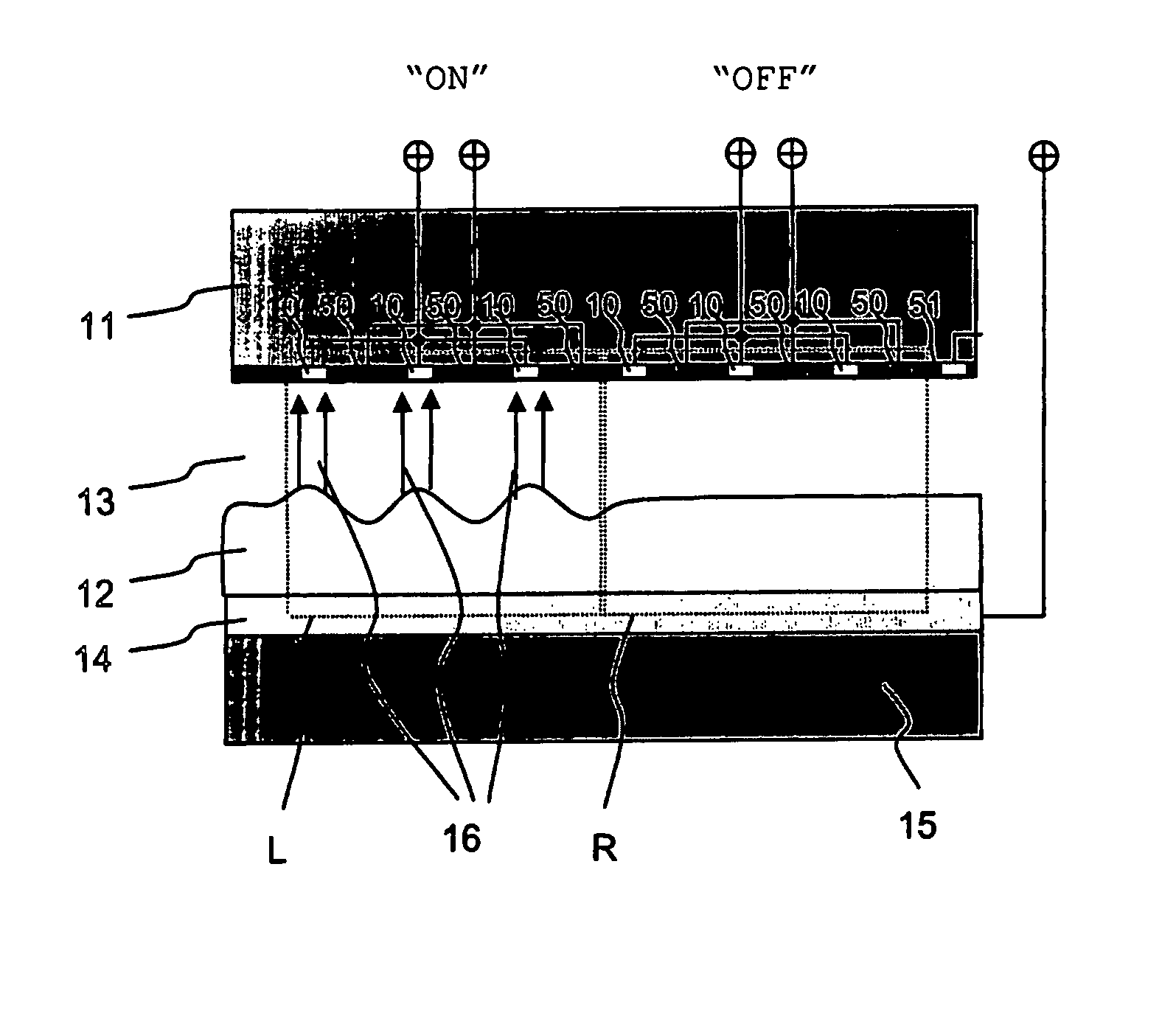
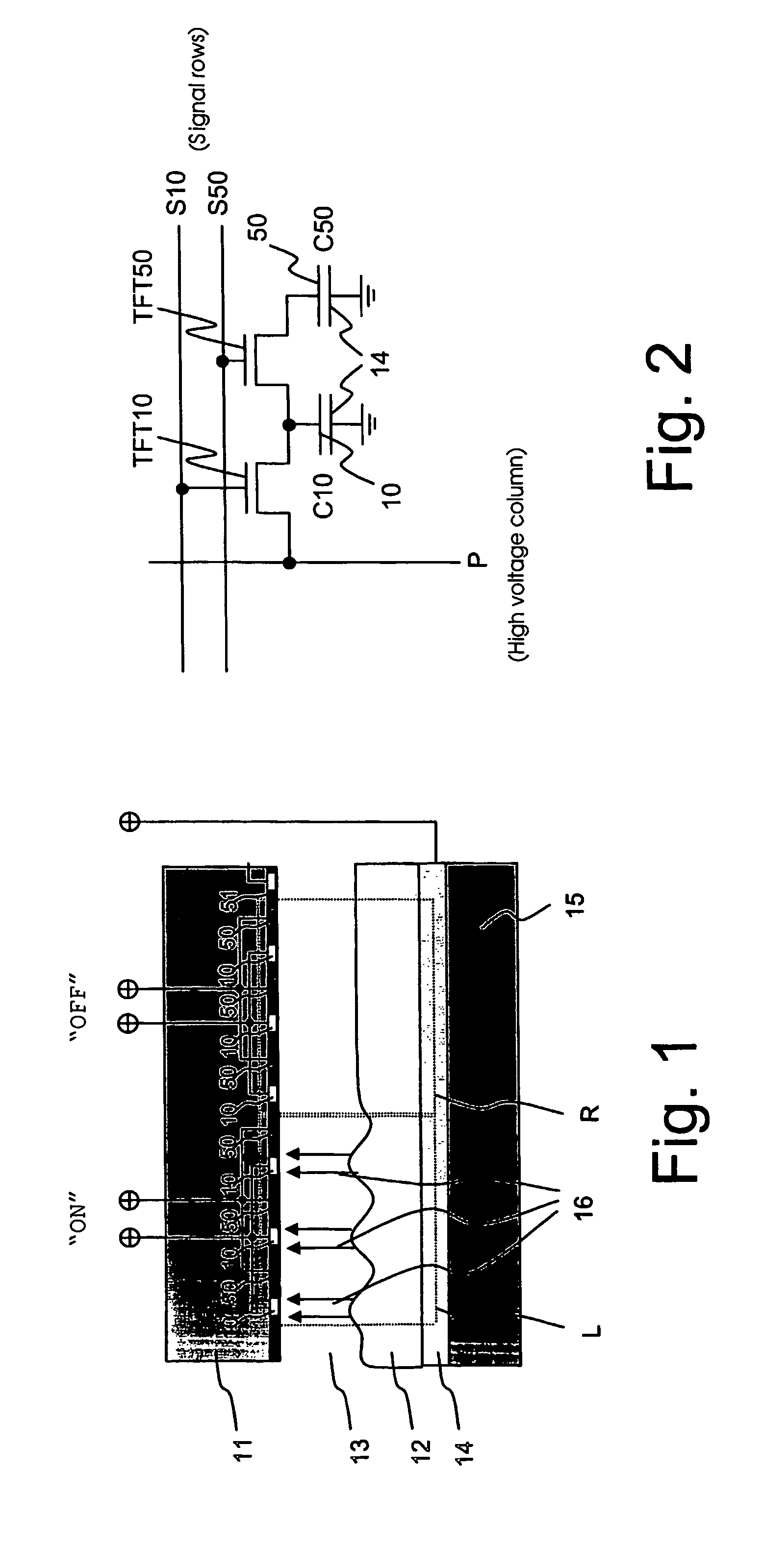
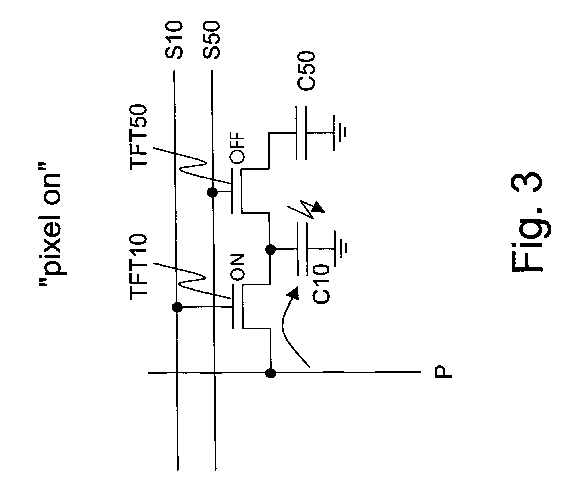
[0022]In the following, the invention is explained in more detail using as an example an enhancement electrode driving system in an optical cell type display. The most important benefits of the invention compared to the prior art solutions are pointed out.

[0023]Earlier patent application PCT / FI02 / 00512 describes the basic function and the layout of the enhancement electrodes in detail, but does not teach any implementation scheme for driving the enhancement electrodes except the obvious solution using a separate power supply and control. In the following, the main attention is directed to the electrical functioning of the electrode configuration. If necessary, more detailed information regarding to the possible layouts of enhancement, signal, and support electrodes in an optical display device may also be found from the aforementioned earlier application.

[0024]To begin, it has to be pointed out that the signal- and enhancement electrode systems can be regarded as separated capacitor...


PUM

PropertyMeasurementUnit
electric fieldaaaaaaaaaa
electric chargeaaaaaaaaaa
voltageaaaaaaaaaa

Abstract

The invention relates to an electrically controlled device, which device comprises at least one electrically and individually controllable cell (L,R) with at least two separate electrode structures (10,50) arranged within the cell, each of the electrode structures capable of storing electric charges (C10,C50). The device further comprises a charge transfer mechanism (P,S10,S20,TFT10,TFT50) to transfer electric charges in a temporally controlled manner between the at least two separate electrode structures (10,50), and that for at least one of the electrode structures within the cell, the charge transfer mechanism comprises substantially the only means for providing electrical power and / or electrical driving. The invention reduces the power consumption of the electrode structures by use of a new type of in-cell type charge recycling. The invention is especially suitable to be used in light modulator components based on the use of electrically deformable viscoelastic materials.

Description

CROSS REFERENCE TO RELATED APPLICATION[0001]This application is for entry into the U.S. national phase under § 371 for International Application No. PCT / FI03 / 000634 having an international filing date of Aug. 29, 2003, and from which priority is claimed under all applicable sections of Title 35 of the United States Code including, but not limited to, Sections 120, 363 and 365(c).TECHNICAL FIELD [0002]The present invention relates to an electrically controlled cell type device comprising at least one electrically and individually controllable cell with at least two separate electrode structures arranged within the cell, the electrode structures capable of storing electric charges.BACKGROUND OF THE INVENTION [0003]Display panels in the form of array of cells, where individual cells contain electrically deformable material, are known in the art. Patent publication WO 01 / 48531, for example, discloses display panel structures where the cells each comprise two deformable dielectric layers...

Claims


Application Information

Patent Timeline
Patent Type & Authority Patents(United States)
IPC IPC(8): G02B26/00G02B5/00G02B27/00G02F1/37H03C7/00H03D9/00
CPCG09G3/3433H03D9/00G09G2330/023G09G2300/0809
Inventor SCHORPP, MARCUS
Owner NOKIA CORP
Why Eureka
Try Eureka