Functional block level clock-gating within a graphics processor

a graphics processor and functional block technology, applied in the direction of generating/distributing signals, high-level techniques, instruments, etc., can solve the problems of increasing the need to reduce the power consumption of the on-chip, becoming more difficult to achieve, and exacerbate the power consumption dilemma

Active Publication Date: 2010-09-21
NVIDIA CORP
View PDF27 Cites 48 Cited by
  • Summary
  • Abstract
  • Description
  • Claims
  • Application Information

AI Technical Summary

Problems solved by technology

As the number of transistors within chips (e.g., microprocessor, graphics chips) has increased, the need to reduce on-chip power consumption has increased and has become more difficult to achieve.
The power consumption dilemma is further exacerbated by the increasing use of large, complex chip designs in mobile devices where low-power consumption is critical.
These known clock signal power saving techniques, however, have several drawbacks.
For example, the latency to slow-down, turn-off, and / or turn-on a clock signal to a fixed zone when entering or exiting a power savings mode within a chip can be prohibitively long (e.g., hundreds of clock cycles) and can substantially disrupt data processing by the chip.

Method used


Image

  • Functional block level clock-gating within a graphics processor
  • Functional block level clock-gating within a graphics processor
  • Functional block level clock-gating within a graphics processor

Examples


Embodiment Construction

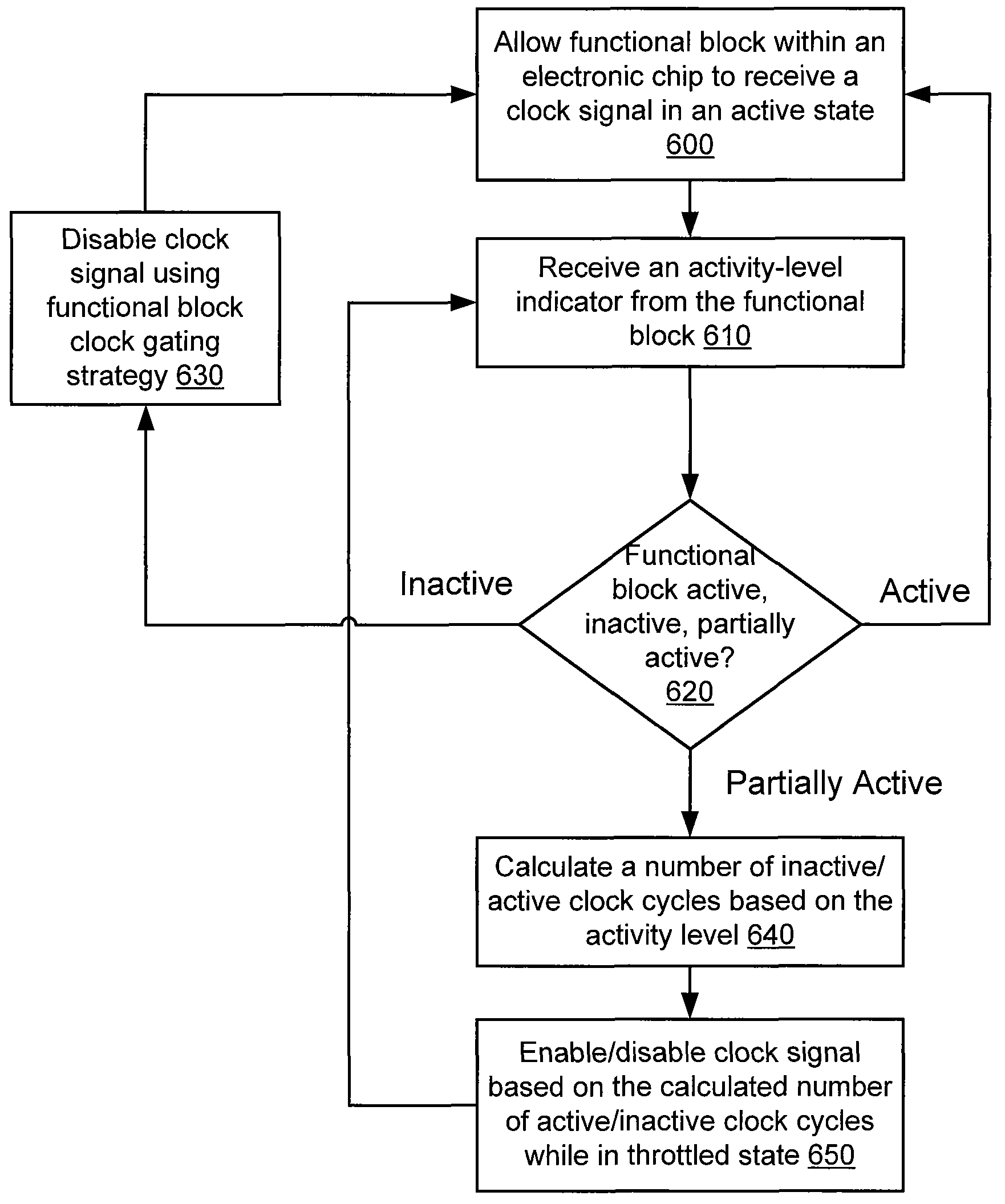
[0020]Clock-gating at a functional block level can be implemented to reduce the overall power consumption of an electronic chip by temporarily disabling (e.g., blocking, turning-off, deactivating) and / or enabling (e.g., unblocking, turning-on, reactivating) a clock signal to a functional block level circuit component within the electronic chip using a clock gate. The functional block level circuit component / unit can be, for example, a functional block, a portion of a functional block and / or an interface circuit between functional blocks in, for example, a data processing pipeline. In some embodiments, the clock signal to a functional block level circuit component can be temporarily disabled, for example, for even just a few clock cycles.

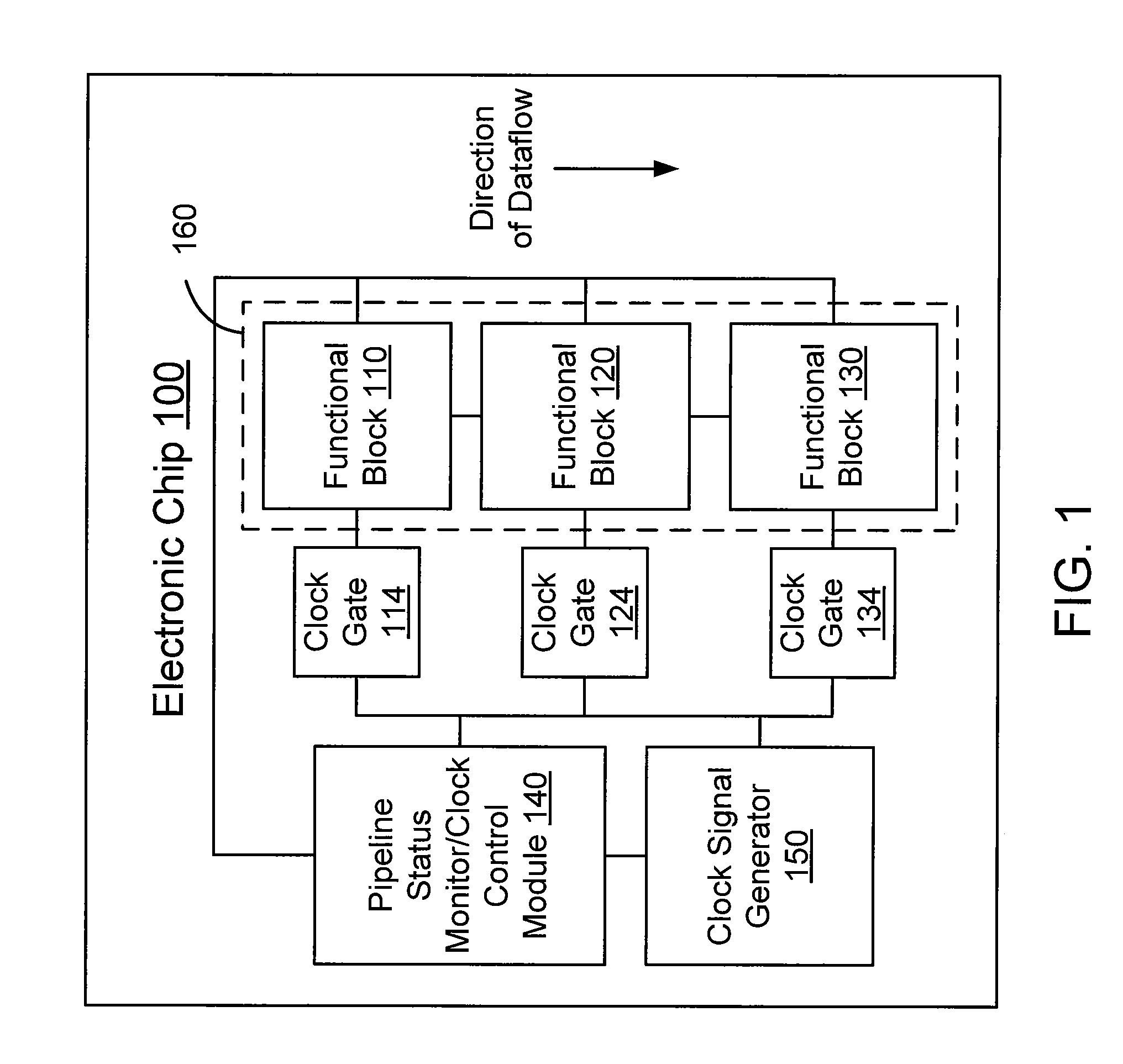
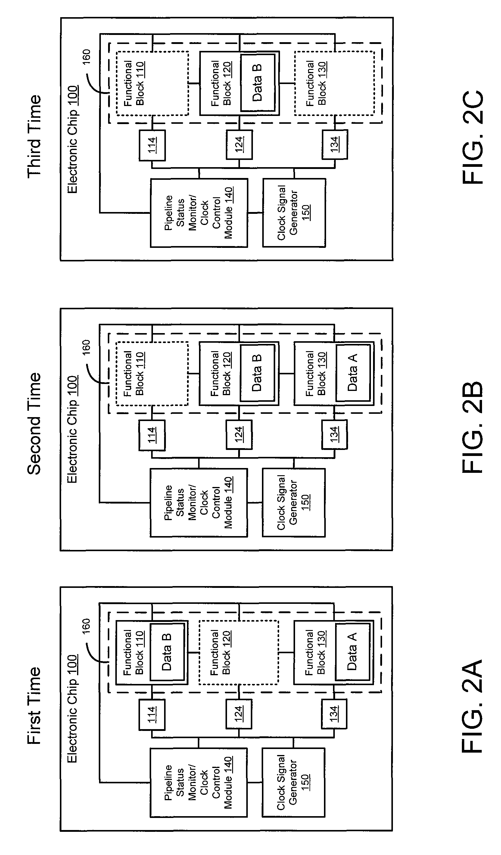
[0021]FIG. 1 is a schematic diagram of an electronic chip 100 configured with a functional block level clock-gating strategy in a data processing pipeline 160, according to an embodiment of the invention. The electronic chip 100 can, for example, be ...


PUM


Abstract

An embodiment of the invention includes receiving an indicator of a flow of data associated with a graphics processing stage within a graphics pipeline of a graphics processor. A clock signal to a portion of the graphics processing stage is modified based on a status of the flow of data. The clock signal is received from a clock signal generator within the graphics processor.

Description

RELATED APPLICATIONS[0001]This application is related to the following commonly owned and assigned applications: application Ser. No. 11 / 614,221, filed on Dec. 21, 2006, now pending, and, application Ser. No. 11,614,236, filed on Dec. 21, 2006, now pending, each of which is incorporated herein by reference in its entirety.BACKGROUND[0002]The disclosed invention relates generally to clock-gating in an electronic chip, and in particular, to functional block level clock-gating.[0003]Managing power consumption within an electronic chip has historically been and continues to be a major factor driving the design of chips within the semiconductor industry. As the number of transistors within chips (e.g., microprocessor, graphics chips) has increased, the need to reduce on-chip power consumption has increased and has become more difficult to achieve. The power consumption dilemma is further exacerbated by the increasing use of large, complex chip designs in mobile devices where low-power co...

Claims


Application Information

Patent Timeline
Patent Type & Authority Patents(United States)
IPC IPC(8): G06F1/32
CPCG06F1/3237G06F1/3203G06F1/08G06F1/3287G06F1/324Y02B60/1217Y02B60/1221Y02B60/32Y02B60/1282Y02B60/1278Y02D10/00Y02D30/50
Inventor ABDALLA, KARIM M.HASSLEN, III, ROBERT J.
Owner NVIDIA CORP
Why Eureka
Try Eureka