Etching method using hard mask in semiconductor device
a hard mask and semiconductor technology, applied in the direction of non-mechanical control, electric permutation locks, lock applications, etc., can solve the problems of large loss generation on the gate hard mask nitride layer, difficult to obtain a vertical cross-sectional profile, etc., to achieve uniform line width and reduce loss
- Summary
- Abstract
- Description
- Claims
- Application Information
AI Technical Summary
Benefits of technology
Problems solved by technology
Method used
Image
Examples
Embodiment Construction
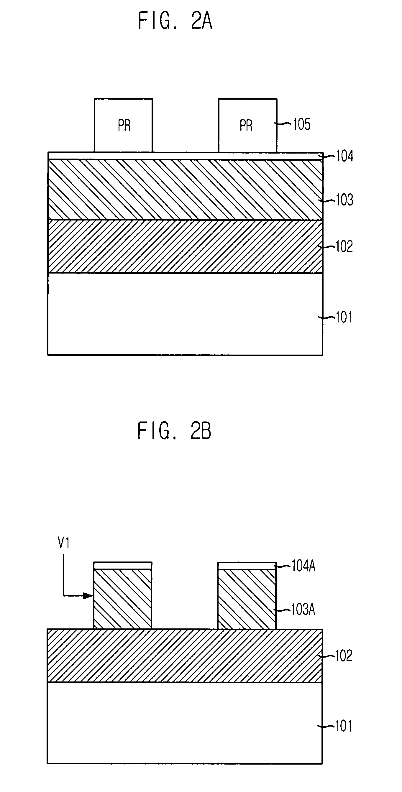
[0016]FIGS. 2A to 2F illustrate an etching method in a semiconductor device in accordance with an embodiment of the present invention. As shown in FIG. 2A, a target etch layer 101 is formed. The target etch layer 101 can include a polysilicon layer or a metal layer. The metal layer can be one selected from a group consisting of tungsten (W), tungsten nitride (WN), tungsten silicide (WSix), titanium (Ti), titanium nitride (TiN), and titanium silicide (TiSix).
[0017]A nitride-based first hard mask layer 102 is formed over the target etch layer 101. A carbon-based second hard mask layer 103 is formed over the first hard mask layer 102. For instance, the first hard mask layer 102 is a silicon nitride (Si3N4) layer, and the second hard mask layer 103 is an amorphous carbon layer.
[0018]An anti-reflective coating layer 104 is formed over the second hard mask layer 103. Then, a photoresist layer (not shown) is formed over the anti-reflective coating layer 104. Then, a photo-exposure and deve...
PUM
| Property | Measurement | Unit |
|---|---|---|
| density | aaaaa | aaaaa |
| flow rate | aaaaa | aaaaa |
| height | aaaaa | aaaaa |
Abstract
Description
Claims
Application Information


