Etching method using hard mask in semiconductor device

a hard mask and semiconductor technology, applied in the direction of non-mechanical control, electric permutation locks, lock applications, etc., can solve the problems of large loss generation on the gate hard mask nitride layer, difficult to obtain a vertical cross-sectional profile, etc., to achieve uniform line width and reduce loss

Inactive Publication Date: 2008-07-03
SK HYNIX INC
View PDF9 Cites 7 Cited by
  • Summary
  • Abstract
  • Description
  • Claims
  • Application Information

AI Technical Summary

Benefits of technology

[0008]Embodiments of the present invention are directed toward providing an etching method in a semiconductor device capable of obtaining a vertical profile by reducing a loss on a hard mask during an etching process, and securing a uniform line width.

Problems solved by technology

Accordingly, it is difficult to obtain a vertical cross-sectional profile since the deposition thickness of the gate hard mask nitride layer is large during etching the gate hard mask nitride layer.
In this case, since an etch selectivity of the fluorine-based etch gas is low to the gate hard mask nitride layer, a large loss may be generated on the gate hard mask nitride layer.

Method used


Image

  • Etching method using hard mask in semiconductor device
  • Etching method using hard mask in semiconductor device
  • Etching method using hard mask in semiconductor device

Examples


Embodiment Construction

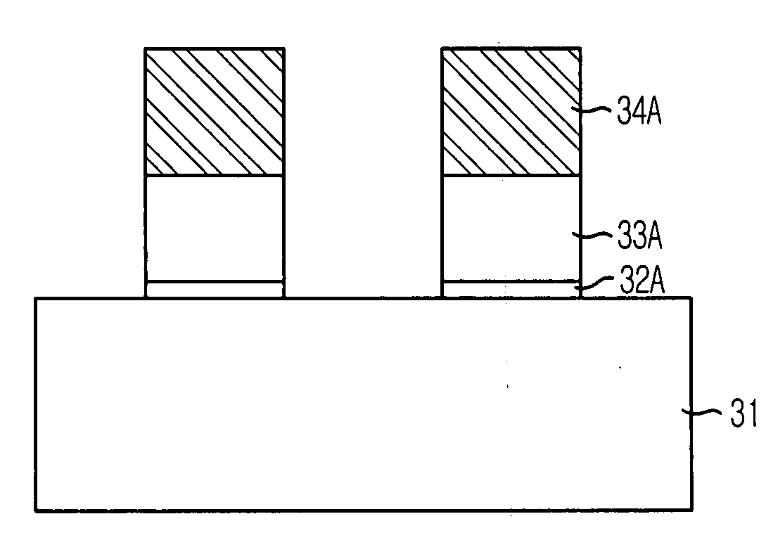
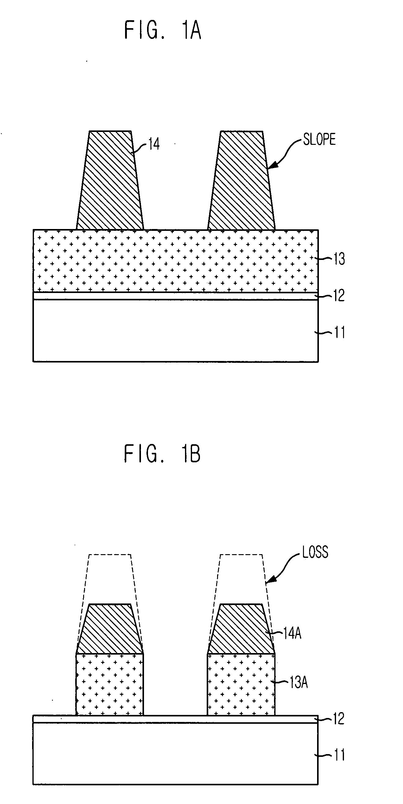
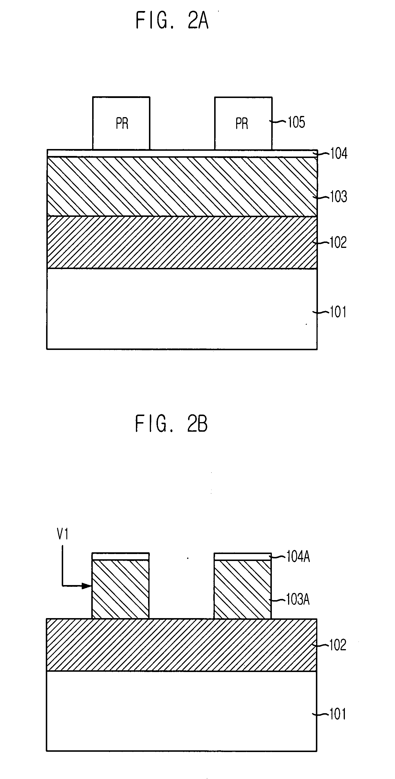
[0016]FIGS. 2A to 2F illustrate an etching method in a semiconductor device in accordance with an embodiment of the present invention. As shown in FIG. 2A, a target etch layer 101 is formed. The target etch layer 101 can include a polysilicon layer or a metal layer. The metal layer can be one selected from a group consisting of tungsten (W), tungsten nitride (WN), tungsten silicide (WSix), titanium (Ti), titanium nitride (TiN), and titanium silicide (TiSix).

[0017]A nitride-based first hard mask layer 102 is formed over the target etch layer 101. A carbon-based second hard mask layer 103 is formed over the first hard mask layer 102. For instance, the first hard mask layer 102 is a silicon nitride (Si3N4) layer, and the second hard mask layer 103 is an amorphous carbon layer.

[0018]An anti-reflective coating layer 104 is formed over the second hard mask layer 103. Then, a photoresist layer (not shown) is formed over the anti-reflective coating layer 104. Then, a photo-exposure and deve...


PUM

PropertyMeasurementUnit
densityaaaaaaaaaa
flow rateaaaaaaaaaa
heightaaaaaaaaaa

Abstract

An etching method in a semiconductor device includes forming a nitride-based first hard mask layer over a target etch layer, forming a carbon-based second hard mask pattern over the first hard mask layer, etching the first hard mask layer using the second hard mask pattern as an etch barrier to form a first hard mask pattern, cleaning a resultant structure including the first hard mask pattern, and etching the target etch layer using the second hard mask pattern as an etch barrier.

Description

CROSS-REFERENCE TO RELATED APPLICATIONS[0001]The present invention claims priority of Korean patent application number 10-2007-0000748, filed on Jan. 3, 2007 which is incorporated by reference in its entirety.BACKGROUND OF THE INVENTION[0002]The present invention relates to a method for fabricating a semiconductor device, and more particularly, to an etching method using a hard mask in a semiconductor device.[0003]For a gate formation in a semiconductor device fabrication process, as a pattern size has been reduced, a loss of a gate hard mask nitride layer has been increased during performing a gate etching method and a landing plug contact etching method. A height of a gate hard mask nitride layer which is finally remaining after etching the landing plug contact to prevent a self aligned contact (SAC) fail has been increased, and a deposition thickness of the gate hard mask nitride layer has been increased as well. Accordingly, it is difficult to obtain a vertical cross-sectional p...

Claims


Application Information

Patent Timeline
Patent Type & Authority Applications(United States)
IPC IPC(8): H01L21/311
CPCH01L21/0206H01L21/28123H01L21/32139H01L21/32137H01L21/32136E05B17/2003E05B47/0012E05B49/00E05B65/025
Inventor YU, JAE-SEONOH, SANG-ROK
Owner SK HYNIX INC
Why Eureka
Try Eureka