Photomask, semiconductor device, and method for manufacturing semiconductor device

a technology of semiconductor devices and masks, applied in the direction of semiconductor devices, instruments, photomechanical treatment, etc., can solve the problems of low dielectric strength of semiconductor elements, reduced uniformity of line width and thickness of resist layers, and difficulty in controlling light intensity applied to boundary zones

Inactive Publication Date: 2011-05-10
SEIKO EPSON CORP
View PDF10 Cites 5 Cited by
  • Summary
  • Abstract
  • Description
  • Claims
  • Application Information

AI Technical Summary

Benefits of technology

[0010]Since the light-blocking section is disposed between the light intensity difference section and the light-transmissive region, light leaking from or reflected by the light-transmissive region can be absorbed by a portion of a resist layer that corresponds to the light-blocking section when the resist layer is exposed to light through the photomask. In other words, unnecessary light can be prevented from entering a portion of the resist layer that corresponds to the light intensity difference section. Therefore, the portion of the resist layer that corresponds to the light intensity difference section can be subjected to light exposure without varying the intensity of light and therefore can be patterned so as to provide a regular line width. This allows a semiconductor layer, which is located under the resist layer and is patterned using the resist layer as a mask, to have a regular width and a regular margin, thereby securing the dielectric strength of a semiconductor element. The resist layer is capable of providing a uniform line width; hence, an impurity can be implanted into a regular portion of the semiconductor layer such that an LDD structure is formed. The light-blocking section covers a necessary portion only, which leads to a reduction in manufacturing cost.
[0024]According to this method, the semiconductor device is manufactured using the photomask; hence, the semiconductor layer can be patterned so as to have a regular line width. This is effective in securing the dielectric strength of a semiconductor element and allows the LDD structure to well function.

Problems solved by technology

In other words, it is difficult to control the intensity of light applied to the boundary zone.
This reduces the uniformity of the line width and thickness of the resist layer.
This causes a problem in that a semiconductor element has low dielectric strength.
Therefore, even if an LDD structure is formed, there is a problem in that the LDD structure malfunctions because the portion X heavily doped with the impurity is in contact with a channel region 114.

Method used


Image

  • Photomask, semiconductor device, and method for manufacturing semiconductor device
  • Photomask, semiconductor device, and method for manufacturing semiconductor device
  • Photomask, semiconductor device, and method for manufacturing semiconductor device

Examples


Embodiment Construction

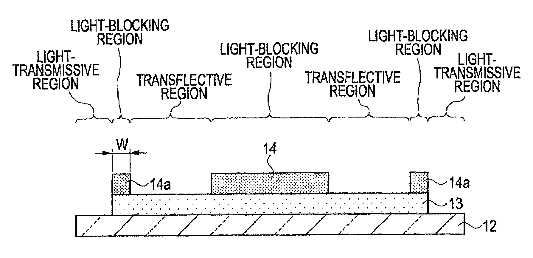
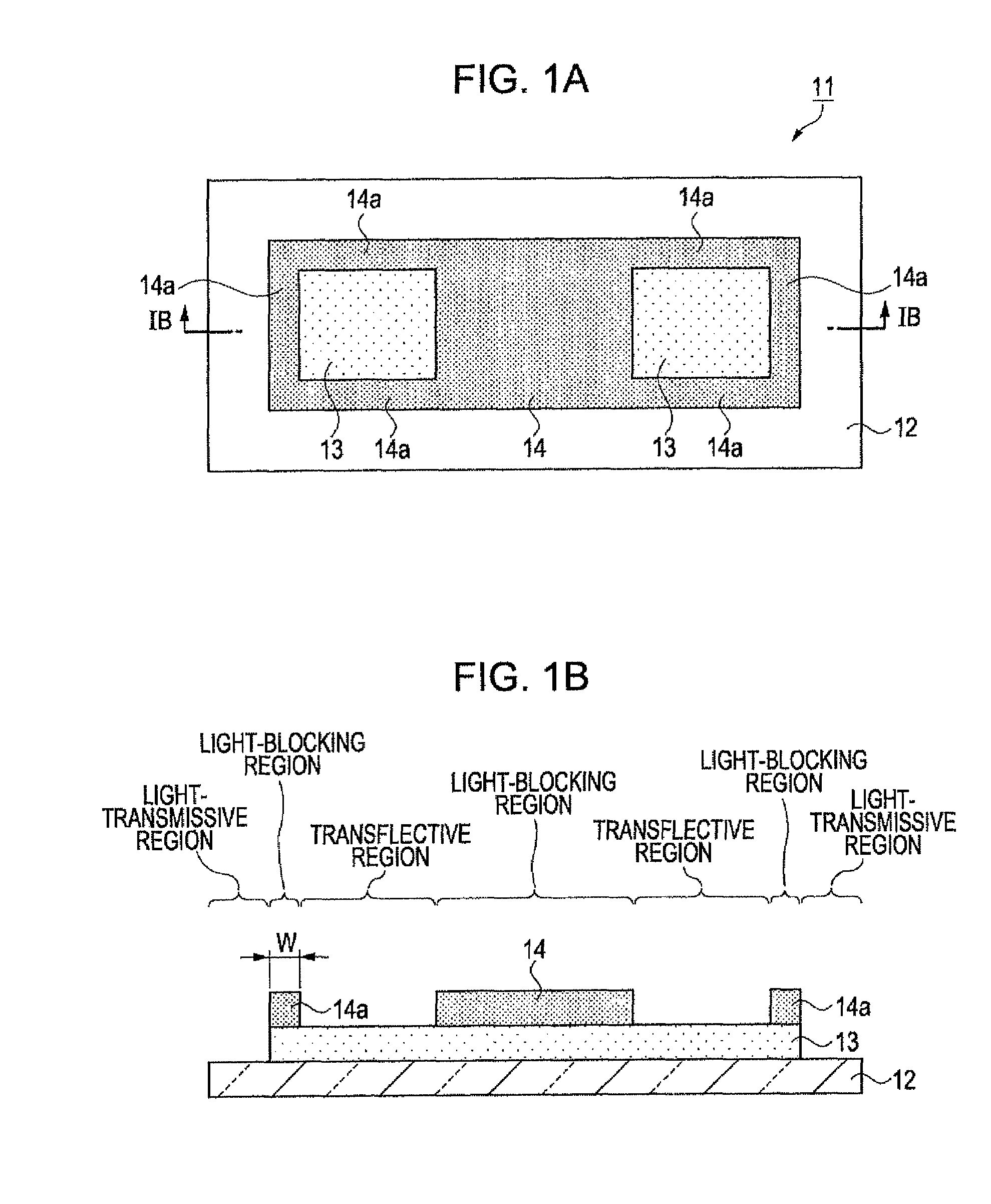
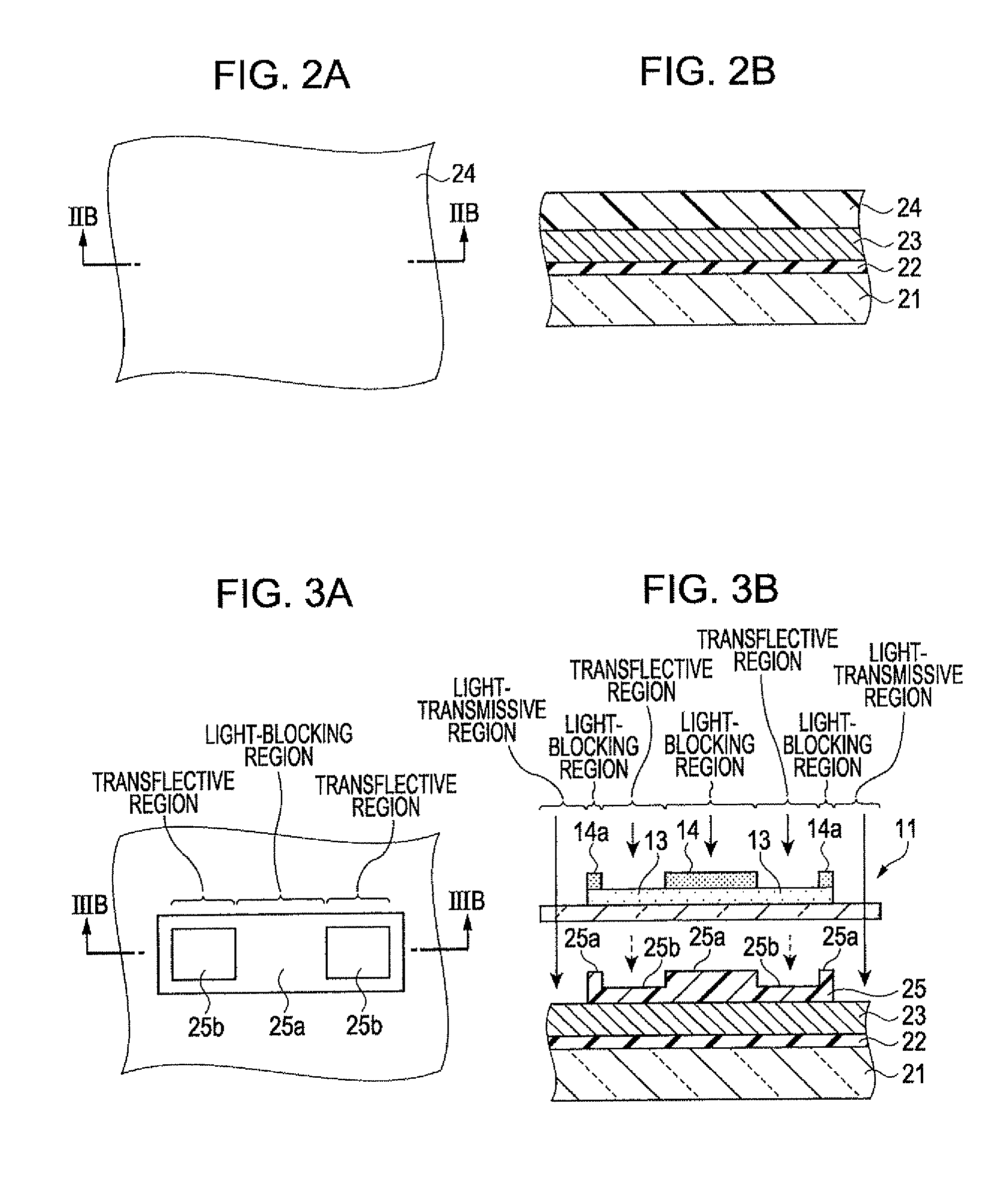
[0046]FIG. 1A is a schematic plan view of a photomask 11 according to an embodiment of the present invention. FIG. 1B is a schematic sectional view of the photomask 11 taken along the line IB-IB. The configuration of the photomask 11 will now be described with reference to FIGS. 1A and 1B.

[0047]With reference to FIGS. 1A and 1B, the photomask 11 includes a mask substrate 12, a transflective layer 13 serving as a light intensity difference section adjusting the transmittance of exposure light emitted from a exposure system (not shown), and a light-blocking layer 14 serving as a light-blocking section that substantially completely blocks light. The photomask 11 is hereinafter referred to as “halftone mask 11”. The mask substrate 12 is made of a transparent material such as glass.

[0048]The transflective layer 13 is disposed on the mask substrate 12 and is made of tantalum oxide (TaO), chromium oxide (CrO), or the like. The transflective layer 13 can be controlled in transmittance (shad...


PUM

PropertyMeasurementUnit
widthaaaaaaaaaa
transmittanceaaaaaaaaaa
thicknessaaaaaaaaaa

Abstract

A photomask includes a light-blocking section that blocks light and also includes a light intensity difference section that controls the intensity of light. The light-blocking section is disposed between the light intensity difference section and a light-transmissive region transmitting light.

Description

BACKGROUND[0001]1. Technical Field[0002]The present invention relates to a photomask having a halftone region, a semiconductor device manufactured using the photomask, and a method for manufacturing the semiconductor device.[0003]2. Related Art[0004]A semiconductor device is manufactured by the following procedure: for example, a semiconductor layer is formed on a substrate and a resist layer is formed on the semiconductor layer and then processed using a halftone photomask so as to have steps as described in JP-A-2006-54424.[0005]In particular, the photomask has a light-blocking region completely blocking light, a transflective region reducing the intensity of light, and a light-transmissive region transmitting light. The resist layer is exposed to light through the photomask, whereby the following portions are formed in the resist layer: a thick portion corresponding to a channel region and thin portions each corresponding to a source region or a drain region.[0006]The semiconduct...

Claims


Application Information

Patent Timeline
Patent Type & Authority Patents(United States)
IPC IPC(8): G03F1/00G03F7/00G03F1/68H01L21/027H01L21/336H01L29/423H01L29/49H01L29/786
CPCG03F1/144G03F1/50G03F1/32G03F1/36
Inventor SERA, HIROSHIMIYATA, TAKASHI
Owner SEIKO EPSON CORP
Why Eureka
Try Eureka