AI technical title is built by Patsnap AI team. It summarizes the technical point description of the patent document.
a technology of semiconductors and substrates, applied in the direction of insulating substrate metal adhesion improvement, conductive pattern formation, printed element electric connection formation, etc., can solve the problem of reducing the non-uniformity of plating current density, reduce the contiguous conductive area of the land, reduce the cost of plating, and reduce the effect of dimpling
Inactive Publication Date: 2009-03-10
AMKOR TECH SINGAPORE HLDG PTE LTD
View PDF126 Cites 5 Cited by
Summary
Abstract
Description
Claims
Application Information
AI Technical Summary
This helps you quickly interpret patents by identifying the three key elements:
Problems solved by technology
Method used
Benefits of technology
Benefits of technology
[0010]The above objectives of reducing or eliminating dimpling and reducing plating cost are provided in a substrate and method for manufacturing a substrate. The substrate incorporates land feature shapes that reduce the contiguous conductive area of the land, thus reducing non-uniformity in the plating current density used to deposit conductive material during a plate-up process and the etching current density used to remove conductive material from above the substrate in a subsequent planarization process. The land shapes further decrease the amount of plating material required in subsequent plating operations that add precious metals for solderability and environmental protection.
[0011]The land shapes include sub-features such as interconnected lines or other interconnected geometric shapes that provide full land functionality, while reducing the area of the feature. The sub-features employed may be designed so that the line width of each sub-feature is the same as the line width of conductive patterns on the substrate, so that the etching process can be made completely or nearly completely uniform. A grid pattern may be employed, so that all of the sub-features intersect (providing electrical interconnection) while maintaining a uniform line width. Alternatively, in particular for circular features such as solderball lands, the features may be rings or ring segments interconnected by segments of conductor, or may be other geometric shapes interconnected by segments of conductor, so that a larger attach area is provided, while reducing plating / etching current density for the land, eliminating or reducing the dimpling effect. The above-described features may also be employed to reduce the cost of subsequent plating operations such as gold or gold-nickel plating, as less material must be deposited on the lands of the present invention than on typical solid lands, thus reducing the plating cost.
Problems solved by technology
The substrate incorporates land feature shapes that reduce the contiguous conductive area of the land, thus reducing non-uniformity in the plating current density used to deposit conductive material during a plate-up process and the etching current density used to remove conductive material from above the substrate in a subsequent planarization process.
Method used
Image
Click on the blue label to locate the original text in one second.
Reading with bidirectional positioning of images and text.
Examples
Embodiment Construction
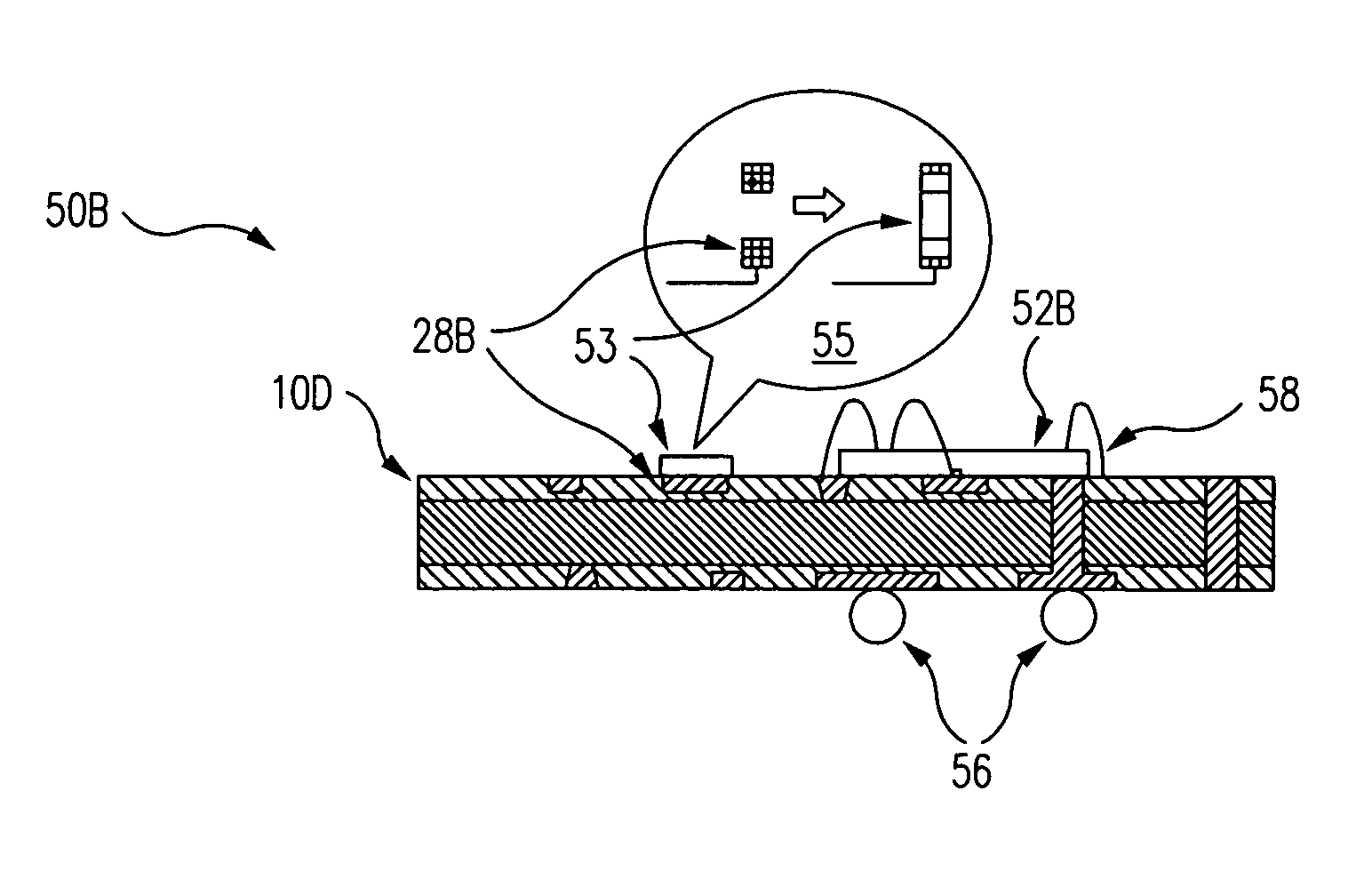
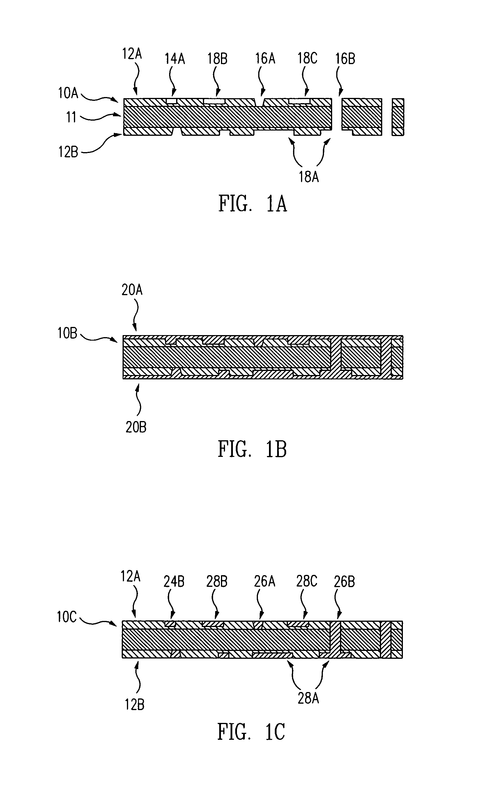
[0020]Referring now to the figures and in particular to FIGS. 1A-1C, a cross-sectional view of stages of preparation of a substrate in accordance with an embodiment of the present invention is shown. A first substrate stage 10A, having a dielectric top layer 12A, a dielectric bottom layer 12B and an optional core 11, which may be a metal ground plane layer or an insulating core, is prepared in accordance with techniques disclosed in the above-incorporated patent applications. Core 11 may be absent, in which case a single dielectric layer may be prepared on one or both sides in accordance with techniques disclosed in the above-incorporated patent applications.
[0021]Substrate stage 10A includes laser-cut or imprinted channels and other features including circuit pattern channels 14A, blind vias 16A, through vias 16B, and features for providing various lands 18A-18C. The present invention concerns the formation and shapes of land features 18A-18C so that dimpling is prevented or reduce...
PUM
Abstract
An integrated circuit substrate having embedded lands with etching and plating control features provides improved manufacture of a high-density and low cost mounting and interconnect structure for integrated circuits. The integrated circuit substrate is formed by generating channels in a dielectric material, adding conductive material to fill the channels and then planarizing the conductive material, so that conductors are formed beneath the surface of the dielectric material. Lands are formed with feature shapes that reduce a dimpling effect at etching and / or an over-deposit of material during plating, both due to increased current density at the relatively larger land areas. Feature shapes may be a grid formed with line sizes similar to those employed to form conductive interconnects, so that all features on the substrate have essentially the same line width. Alternatively, and in particular for circular pads such as solderball attach lands, sub-features may be radially disposed around a central circular area and connected with channels formed as interconnect lines that connect the sub-features to the central circular area. Connection of the lands may be made using vias or by other conductive channels forming electrical interconnect lines.
Description
CROSS-REFERENCE TO RELATED APPLICATIONS[0001]This application is a divisional of U.S. patent application Ser. No. 10 / 701,782, filed on Nov. 5, 2003, entitled “INTEGRATED CIRCUIT SUBSTRATE HAVING EMBEDDED LANDS WITH ETCHING AND PLATING CONTROL SHAPES”, which is a continuation-in-part of the following U.S. patent applications: 1) “IMPRINTED INTEGRATED CIRCUIT SUBSTRATE AND METHOD FOR IMPRINTING AN INTEGRATED CIRCUIT SUBSTRATE”, U.S. patent application Ser. No. 09 / 884,193, filed Jun. 19, 2001, and issued as U.S. Pat. No. 6,967,124 on Nov. 22, 2005; 2) “INTEGRATED CIRCUIT SUBSTRATE HAVING LASER-EMBEDDED CONDUCTIVE PATTERNS AND METHOD THEREFOR”, U.S. patent application Ser. No. 10 / 138,225, filed May 1, 2002, and issued as U.S. Pat. No. 6,930,256 on Aug. 16, 2005; 3) “SOLDERABLE INJECTION-MOLDED INTEGRATED CIRCUIT SUBSTRATE AND METHOD THEREFOR”, U.S. patent application Ser. No. 09 / 931,144, filed Aug. 16, 2001, and issued as U.S. Pat. No. 6,784,376 on Aug. 31, 2004; and 4) “INTEGRATED CIRC...
Claims
Application Information
Patent Timeline
Application Date:The date an application was filed.
Publication Date:The date a patent or application was officially published.
First Publication Date:The earliest publication date of a patent with the same application number.
Issue Date:Publication date of the patent grant document.
PCT Entry Date:The Entry date of PCT National Phase.
Estimated Expiry Date:The statutory expiry date of a patent right according to the Patent Law, and it is the longest term of protection that the patent right can achieve without the termination of the patent right due to other reasons(Term extension factor has been taken into account ).
Invalid Date:Actual expiry date is based on effective date or publication date of legal transaction data of invalid patent.

