

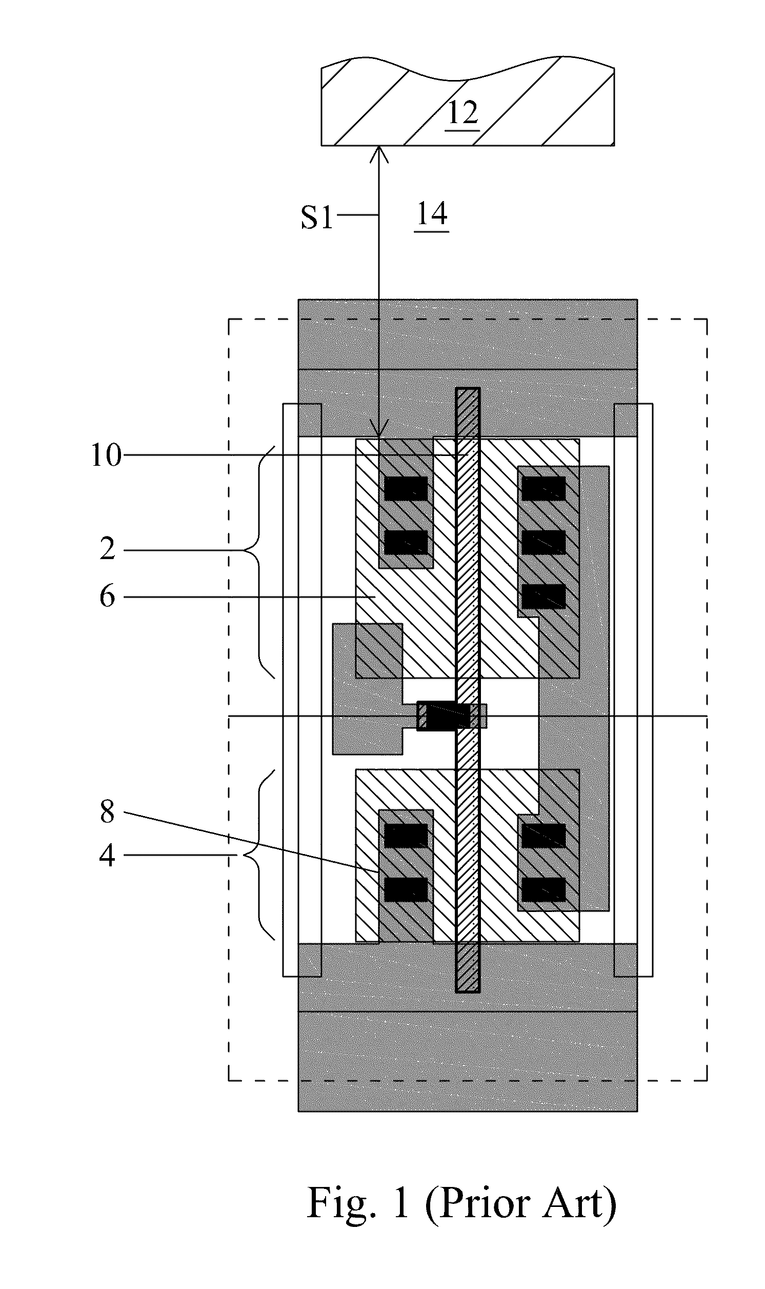
Standard cell without OD space effect in Y-direction
a technology of od space and standard cell, applied in the direction of basic electric elements, semiconductor devices, electrical equipment, etc., can solve the problems of significant variation of affecting the and affecting the drive current of the respective mos device to a degree not acceptable to certain design, so as to achieve the effect of more predictable performance of the mos devi
- Summary
- Abstract
- Description
- Claims
- Application Information
AI Technical Summary
Benefits of technology
Problems solved by technology
Method used
Image

Examples
Embodiment Construction
[0021]The making and using of the presently preferred embodiments are discussed in detail below. It should be appreciated, however, that the present invention provides many applicable inventive concepts that can be embodied in a wide variety of specific contexts. The specific embodiments discussed are merely illustrative of specific ways to make and use the invention, and do not limit the scope of the invention.
[0022]Novel integrated circuits including spacer bars for regulating stresses applied on metal-oxide-semiconductor (MOS) devices are presented. The preferred embodiments and the variations of the preferred embodiments are discussed. Throughout the various views and illustrative embodiments of the present invention, like reference numbers are used to designate like elements.
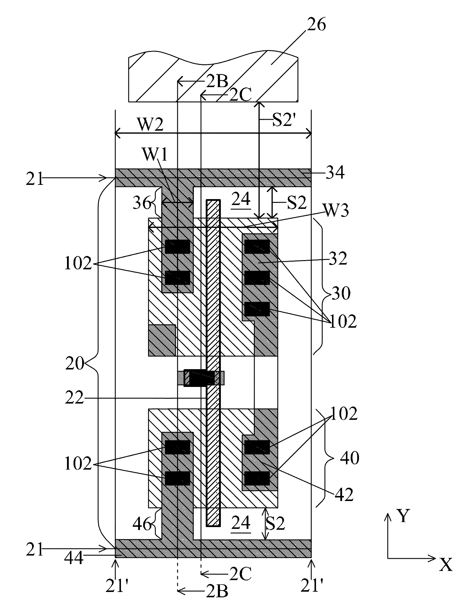
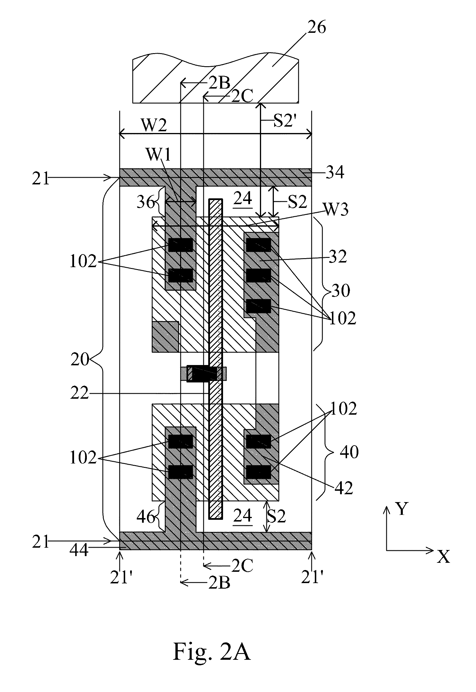
[0023]FIG. 2A illustrates an embodiment of the present invention. A portion of standard cell 20, which has certain logic function, is provided. The illustrated standard cell 20 includes PMOS device 30 and N...
PUM
 Abstract
Description
Claims
Application Information