Methods of forming a ferroelectric layer and methods of manufacturing a ferroelectric capacitor including the same

a technology of ferroelectric capacitor and ferroelectric layer, which is applied in the direction of coating, solid-state device, chemical vapor deposition coating, etc., can solve the problems of poor electrical characteristics of framing devices including the pzt layer, high fatigue and difficulty in forming the upper electrode on the pzt layer, so as to reduce the time for forming and enhance the leakage current characteristics of the pzt layer. , the effect o

Active Publication Date: 2010-10-12
SAMSUNG ELECTRONICS CO LTD
View PDF5 Cites 0 Cited by
  • Summary
  • Abstract
  • Description
  • Claims
  • Application Information

AI Technical Summary

Benefits of technology

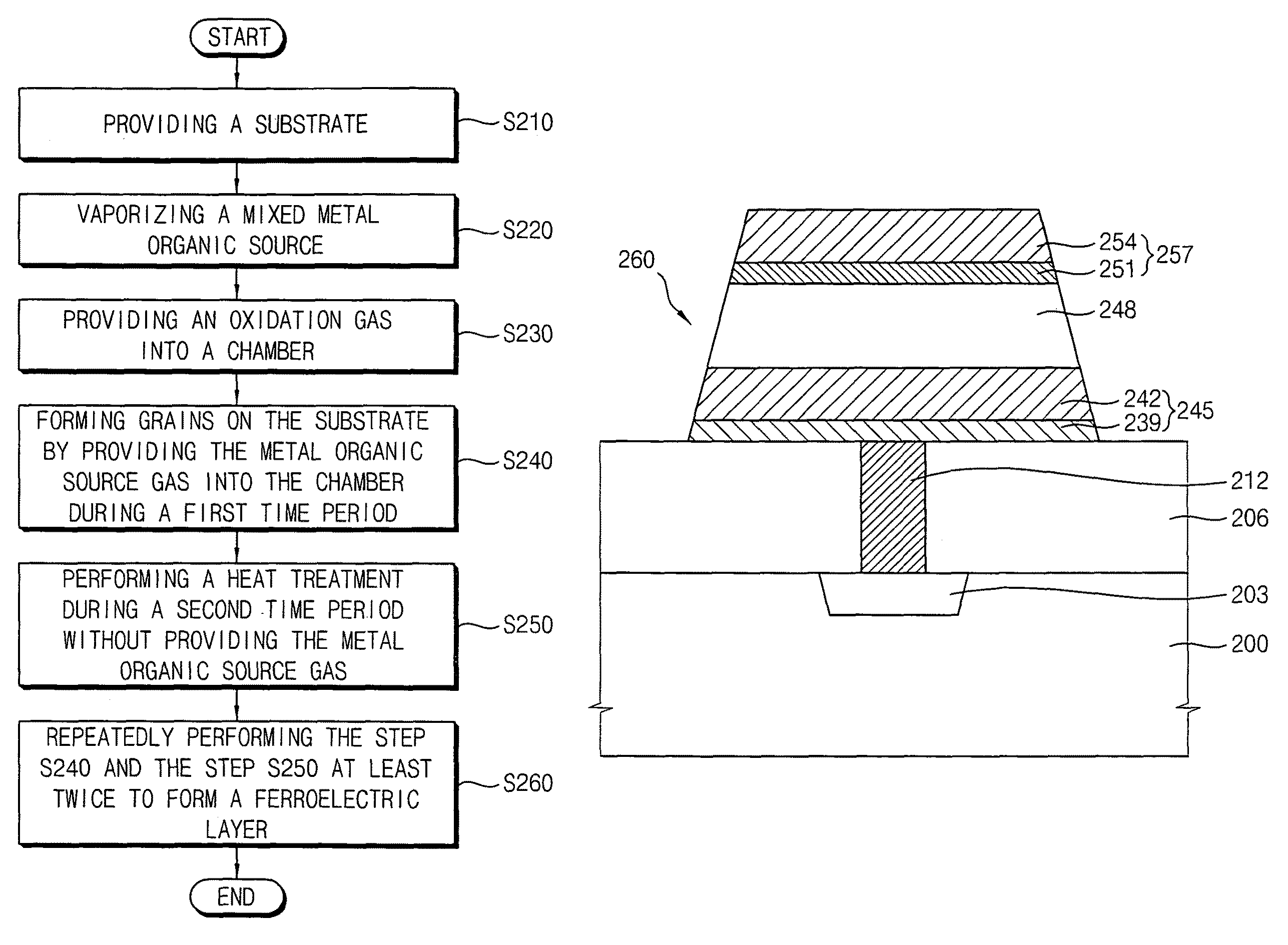
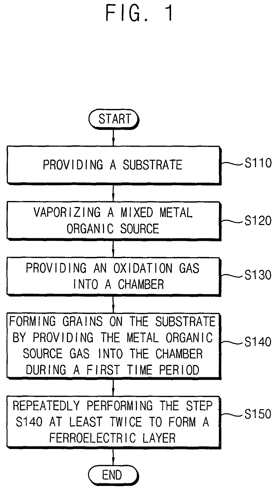
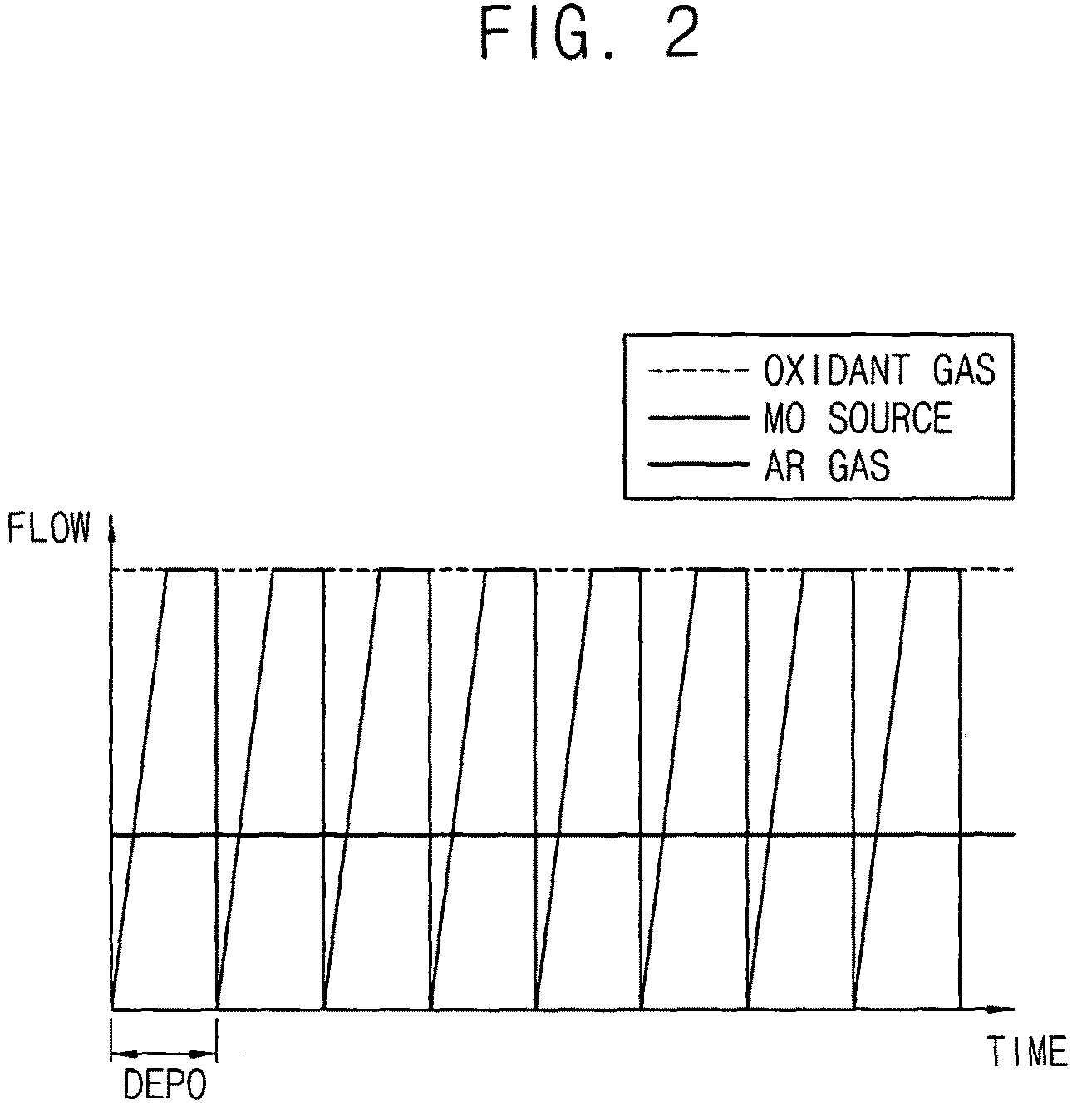
[0016]According to embodiments of the present invention, a chemical vapor deposition (CVD) process including repeatedly providing a gas including at least two different metal-organic sources with intervals into a chamber into which an oxidation gas is provided, so that crystallization occurs at a temperature under 650° C. to form a ferroelectric layer without undesirable defects, by-products or impurities. Thus, ferroelectric properties such as data preservation, polarization maintenance, etc. may be improved or maintained, and enhance leakage current characteristics of the ferroelectric layer. Additionally, electrical properties of a ferroelectric capacitor including the ferroelectric layer described herein may be largely improved. Furthermore, the CVD process according to embodiments of the present invention providing a source gas repeatedly with intervals may reduce the time for forming the ferroelectric layer compared with an atomic layer deposition (ALD) process, so that the CVD process may be applicably suitable for mass production of semiconductor devices.

Problems solved by technology

However, a PZT layer may be highly fatigued when subjected to repeated polarization inversion.
Thus, a FRAM device including the PZT layer may have poor electrical characteristics.
Accordingly, forming the upper electrode on the PZT layer may be complicated, and the upper electrode may be easily detached from the PZT layer.
The defects may deteriorate the electrical characteristics of the FRAM device.
However, at least due to the characteristics of the ALD process, performing the ALD process requires a longer period of time than a CVD process, at least because two purge processes and an oxidation process are required in one cycle of the ALD process for depositing a layer.
Additionally, developing source gases for forming a ferroelectric layer that are suitable for an ALD process is often met with difficulty.

Method used


Image

  • Methods of forming a ferroelectric layer and methods of manufacturing a ferroelectric capacitor including the same
  • Methods of forming a ferroelectric layer and methods of manufacturing a ferroelectric capacitor including the same
  • Methods of forming a ferroelectric layer and methods of manufacturing a ferroelectric capacitor including the same

Examples


Embodiment Construction

[0025]The present invention will now be described more fully with reference to the accompanying drawings, in which exemplary embodiments of the invention are shown. The invention may, however, be embodied in many different forms and should not be construed as being limited to the embodiments set forth herein; rather, these embodiments are provided so that this disclosure will be thorough and complete, and will fully convey the concept of the invention to those skilled in the art. Like reference numerals in the drawings denote like elements, and thus their description will be omitted.

[0026]It will be understood that when an element, such as a layer, is referred to as being “connected to,”“coupled to” or “responsive to” (and / or variants thereof) another element, it can be directly connected, coupled or responsive to the other element or intervening elements may be present. In contrast, when an element is referred to as being “directly connected to,”“directly coupled to” or “directly r...


PUM

PropertyMeasurementUnit
time periodaaaaaaaaaa
temperatureaaaaaaaaaa

Abstract

A method of forming a ferroelectric layer is provided. A metal-organic source gas is provided into a chamber into which an oxidation gas is provided for a first time period to form ferroelectric grains on a substrate. A ferroelectric layer is formed by performing at least twice a step of providing a metal-organic source gas into the chamber during the first time period using a pulse method to grow the ferroelectric grains.

Description

CROSS-REFERENCE TO RELATED PATENT APPLICATIONS[0001]This application claims the benefit of Korean Patent Application No. 10-2007-76678, filed on Jul. 31, 2007, in the Korean Intellectual Property Office, the disclosure of which is incorporated herein by reference in its entirety.FIELD OF THE INVENTION[0002]Embodiments of the present invention relate to methods of forming a ferroelectric layer and methods of manufacturing a ferroelectric capacitor using the same. More particularly, embodiments of the present invention relate to methods of forming a ferroelectric layer by performing a chemical vapor deposition (CVD) process in which a source gas is repeatedly provided, and methods of manufacturing a ferroelectric capacitor using at least similar processes.BACKGROUND OF THE INVENTION[0003]Generally, semiconductor devices may be divided into two categories: volatile semiconductor memory devices and non-volatile semiconductor memory devices. Volatile semiconductor memory devices, such as...

Claims


Application Information

Patent Timeline
Patent Type & Authority Patents(United States)
IPC IPC(8): H01L21/00
CPCC23C16/409C23C16/45523H01L28/56H01L27/105H10B12/00
Inventor IM, DONG-HYUNKIM, IK-SOOLEE, CHOONG-MANHEO, JANG-EUNLEE, SUNG-JU
Owner SAMSUNG ELECTRONICS CO LTD
Why Eureka
Try Eureka