Semiconductor apparatus and method of manufacturing semiconductor apparatus
a technology of semiconductor apparatus and semiconductor material, which is applied in the direction of semiconductor devices, electrical devices, basic electric elements, etc., can solve the problems of increasing on-resistance, increasing on-resistance, and uneven thickness of channels, so as to achieve uniform channel thickness and increase on-resistance
- Summary
- Abstract
- Description
- Claims
- Application Information
AI Technical Summary
Benefits of technology
Problems solved by technology
Method used
Image
Examples
first embodiment
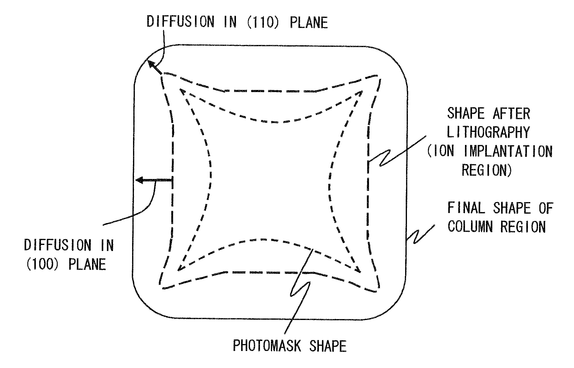
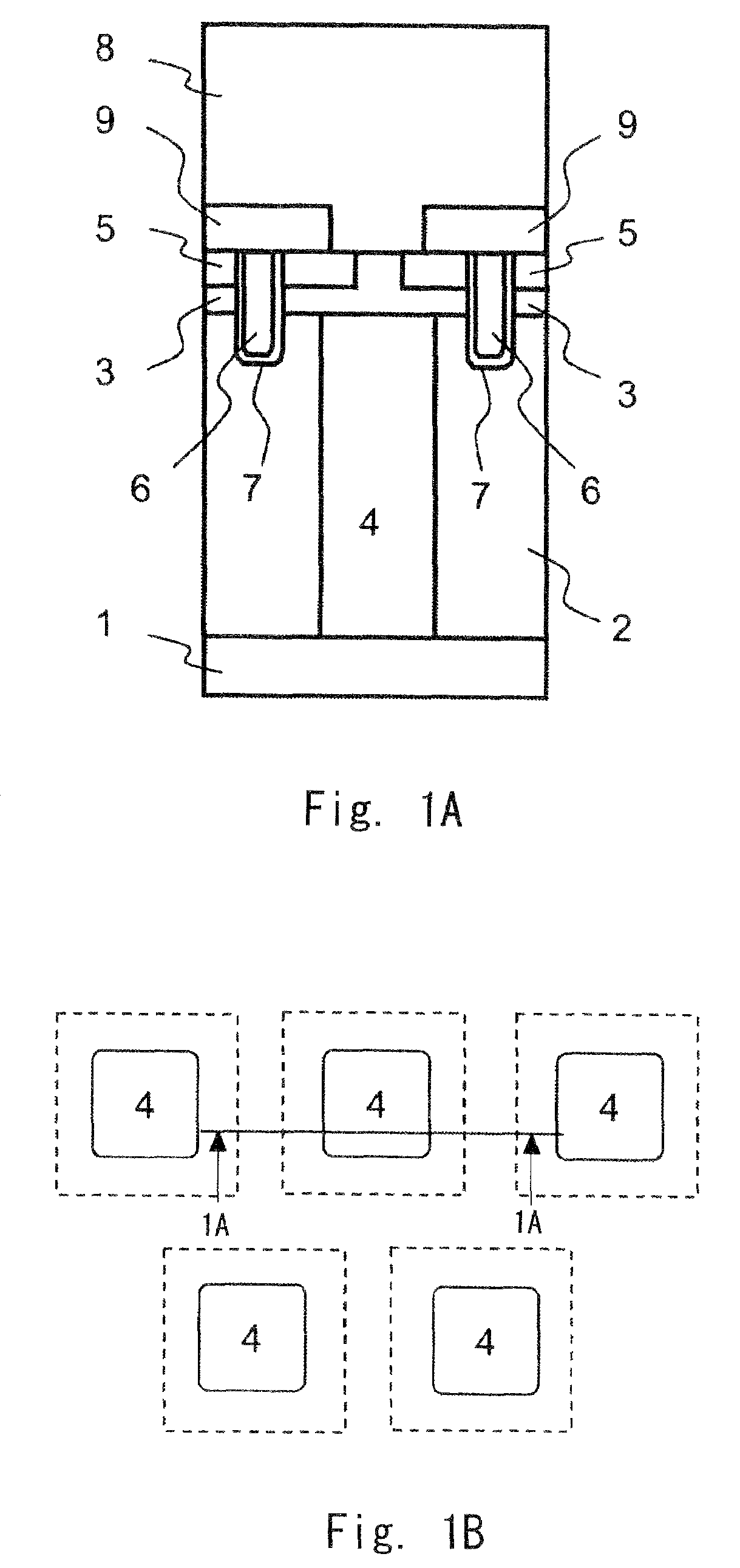
[0027]An exemplary embodiment of the present invention is described hereinafter with reference to the drawings. FIG. 1A is a sectional view of semiconductor apparatus according to a first embodiment of the present invention. FIG. 1B is a plan view of the semiconductor apparatus shown in FIG. 1A. FIG. 1A shows the cross section along line 1A-1A in FIG. 1B.
[0028]A semiconductor substrate 1 shown in FIG. 1 may be an N+ type (first conductivity type) semiconductor substrate which is made of silicon or the like, for example. On the semiconductor substrate 1, a drift region 2 is formed. The drift region 2 may be an N-type (first conductivity type) semiconductor which is made of an epitaxial layer (semiconductor layer) that is formed by epitaxially growing silicon with phosphorus doping, for example. The drift region 2 and the semiconductor substrate 1 serve as the drain of a vertical power MOSFET.
[0029]A base region 3 is formed on the drift region 2. The base region 3 may be a P type (sec...
second embodiment
[0045]FIGS. 5A and 5B show a semiconductor apparatus 200 according to a second embodiment of the present invention. In FIGS. 5A and 5B, the same elements as in FIGS. 1A and 1B are denoted by the same reference numerals and not described in detail herein. The sectional view of the semiconductor apparatus 200 shown in FIG. 5A is the same as the sectional view of the semiconductor apparatus 100 shown in FIG. 1A. In the plan view of the semiconductor apparatus 100 according to the first embodiment shown in FIG. 1B, each column region has a rectangular shape. On the other hand, in the plan view of the semiconductor apparatus 200 according to the second embodiment shown in FIG. 5B, each column region has a hexagonal shape. The distance from the hexagonal column region to the gate insulating film is uniform. A method of forming the column region in a hexagonal shape is described hereinbelow.
[0046]FIG. 6 shows a compensation pattern of a mask when a column region is formed in a hexagonal sh...
PUM
 Abstract
Description
Claims
Application Information


