
Semiconductor device

a technology of semiconductors and insulating films, applied in the direction of semiconductor devices, basic electric elements, electrical appliances, etc., can solve the problem of low reliability of insulating films, and achieve the effect of improving short-circuit withstand capability and increasing on-resistan

Active Publication Date: 2019-06-04
MITSUBISHI ELECTRIC CORP
View PDF19 Cites 0 Cited by
  • Summary
  • Abstract
  • Description
  • Claims
  • Application Information

AI Technical Summary

Benefits of technology

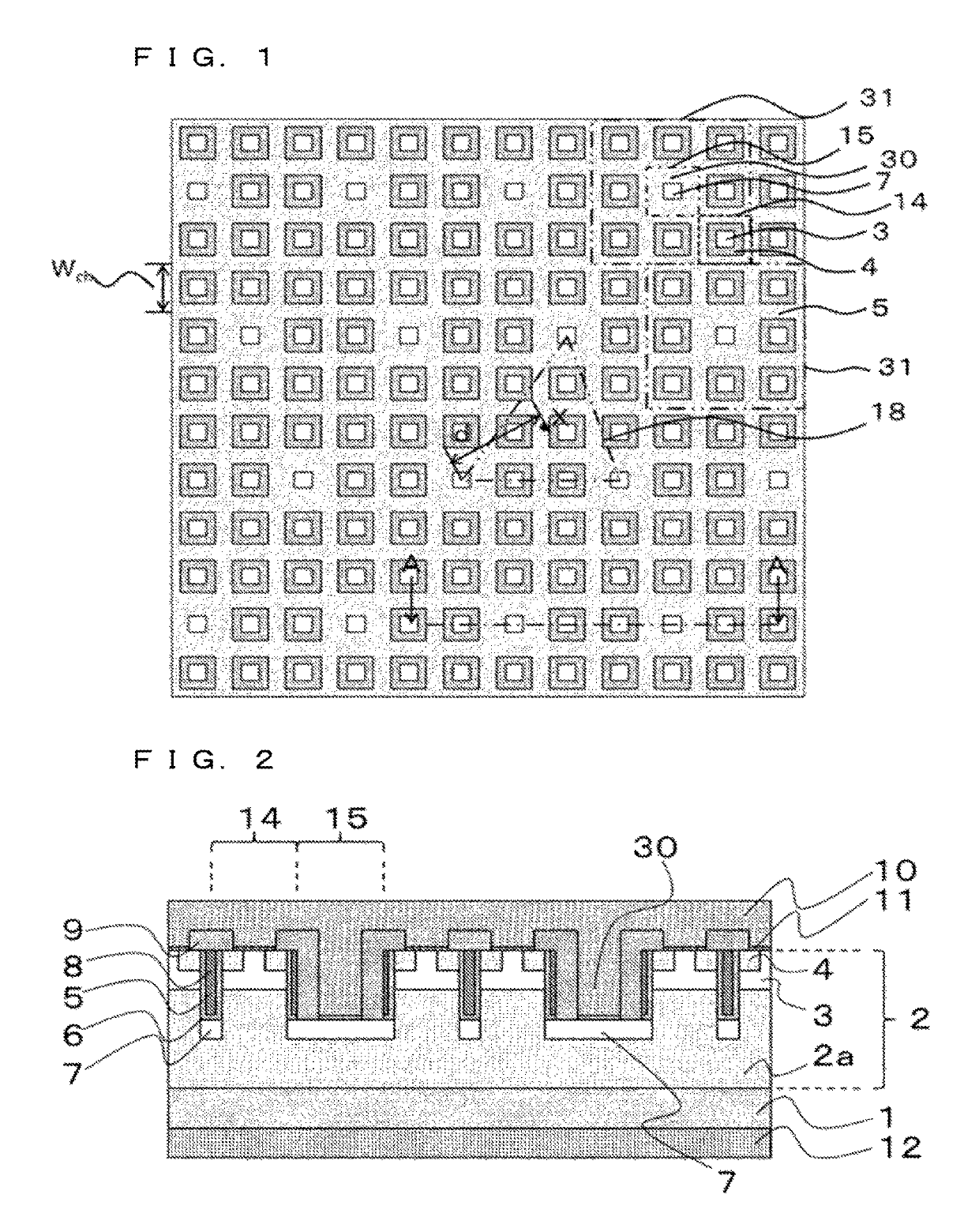
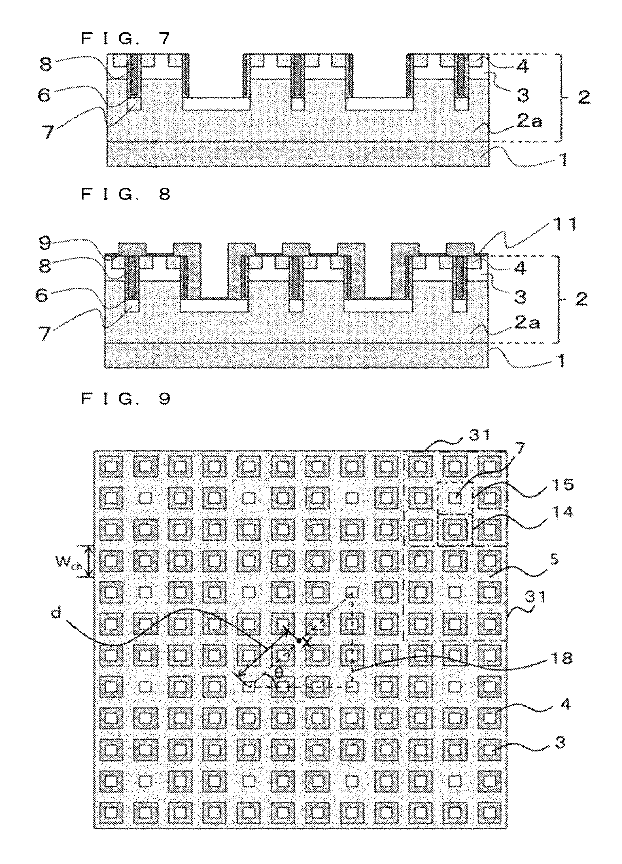
[0011]In the semiconductor device according to the present invention, the protective contact region connecting the protective diffusion layer and the source electrode to each other is disposed such that the triangle, whose vertices are the centers of three protective contact regions located closest to one another, is an acute triangle. Thus, if the same number of protective contact regions are provided, the distance from the protective contact region to a point farthest therefrom can be made smaller than in the case where the protective contact regions are arranged in a lattice pattern. This improves short-circuit withstand capability while restraining an increase in on-resistance.

Problems solved by technology

During the off state of the semiconductor device, an electric field tends to concentrate on an insulating film on the bottom of a trench in the trench MOSFET, on which, the reliability of the insulating film is low.

Method used


Image

  • Semiconductor device
  • Semiconductor device
  • Semiconductor device

Examples


first embodiment

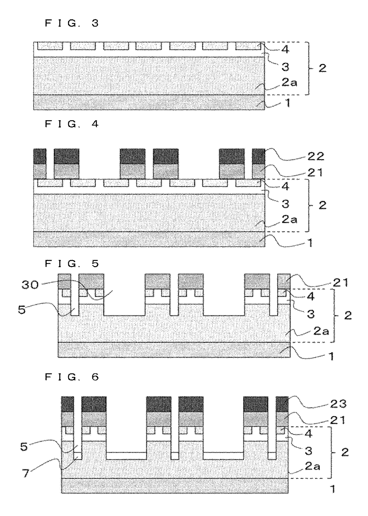
[0031]First, a semiconductor device according to a first embodiment of the present invention will be described. FIG. 1 is a plan view for explaining the semiconductor device according to the first embodiment of the present invention. Illustrated herein as an example of the semiconductor device is a trench gate MOSFET that is a silicon carbide semiconductor device including silicon carbide (SiC).

[0032]The present embodiment is not limited to the description below, and can be modified as appropriate within the scope of the present invention. For easy understanding, the scales of the members may differ from actual ones in the drawings below. The same applies to the scales among the drawings.

[0033]FIG. 1 illustrates a MOSFET region that is part of an active region of the trench gate MOSFET. The MOSFET region is formed of cell regions 14, which are surrounded by dotted lines, and protective contact regions 15, which are surrounded by alternate long and short dashed lines. The cell region...

second embodiment

[0111]FIGS. 16 and 17 are tops views of a semiconductor device according to a second embodiment. The semiconductor device of the present embodiment is characterized in that channel regions remote from the protective contact regions 15 are deactivated. The second embodiment is similar to the first embodiment in the other respects. The present embodiment achieves an effect of improving short-circuit withstand capability.

[0112]With reference to FIGS. 16 and 17, if circles 24 are each drawn around the protective contact region 15, deactivation channels 25 that are caused not to function as MOS channels may be channels located outside the circles 24.

[0113]In this case, the radius of the circle 24 is one or more times and three or less times, desirably, two or less times the width Wch of the cell region 14. This is because an on-resistance increases due to an increase in the ratio of deactivated channels if the radius is smaller than one time the width Wch, and an effect of improving shor...


PUM


Abstract

A semiconductor device includes a base region of second conductivity type formed on a drift layer of first conductivity type, a source region of first conductivity type located in the base region, a trench passing through the base region and the source region and dividing cell regions in plan view, a protective diffusion layer of second conductivity type disposed on a bottom of the trench, a gate electrode embedded in the trench with a gate insulating film therebetween, a source electrode electrically connected to the source region, and a protective contact region disposed at each of positions of three or more cell regions and connecting the protective diffusion layer and the source electrode to each other. The protective contact regions are disposed such that a triangle whose vertices are centers of three protective contact regions located closest to one another is an acute triangle.

Description

TECHNICAL FIELD[0001]The present invention relates to semiconductor devices.BACKGROUND ART[0002]In electronics equipment, insulated gate semiconductor devices, such as insulated gate bipolar transistors (IGBTs) and metal oxide semiconductor field effect transistors (MOSFETs), are widely used as switching elements for controlling power supply to loads such as motors. One example of such an insulated gate semiconductor device is a trench-gate MOSFET in which a gate electrode is embedded in a semiconductor layer.[0003]For example, MOSFET cells (cell regions) connected in parallel are treated as one semiconductor device in a typical vertical MOSFET. In other words, a semiconductor device including a vertical MOSFET is formed by arranging MOSFET cells. Typical examples of the arrangement patterns of MOSFET include a cell pattern and a stripe pattern. In the cell pattern, MOSFET cells each including a square source region surrounded by a gate trench are arranged in a lattice pattern. In t...

Claims


Application Information

Patent Timeline
Patent Type & Authority Patents(United States)
IPC IPC(8): H01L29/66H01L29/417H01L29/739H01L29/06H01L21/04H01L29/16H01L29/10H01L27/02H01L29/78
CPCH01L27/0296H01L21/046H01L21/0475H01L27/0288H01L29/0623H01L29/7813H01L29/1087H01L29/1608H01L29/41766H01L29/7397H01L29/7802H01L29/0696
Inventor SUGAWARA, KATSUTOSHIKAGAWA, YASUHIROTANAKA, RINAFUKUI, YUTAKA
Owner MITSUBISHI ELECTRIC CORP
Learn More