
Power semiconductor device

a technology of semiconductor devices and semiconductors, applied in the field of semiconductor devices, can solve the problems of increasing channel resistance and on resistance, and achieve the effect of reducing saturated current and increasing on resistan

Active Publication Date: 2020-09-01
TOYOTA CENT RES & DEV LAB INC
View PDF2 Cites 0 Cited by
  • Summary
  • Abstract
  • Description
  • Claims
  • Application Information

AI Technical Summary

Benefits of technology

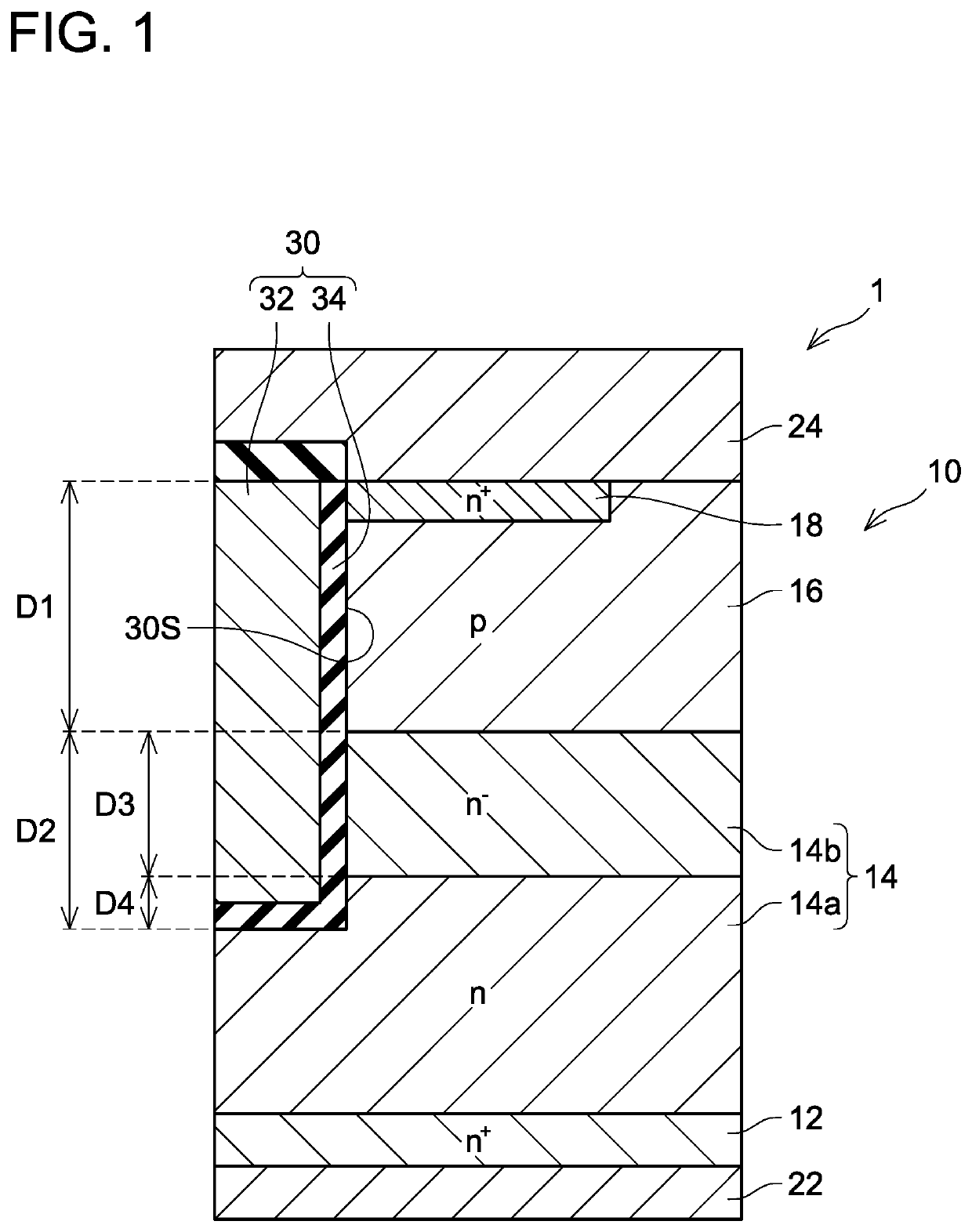
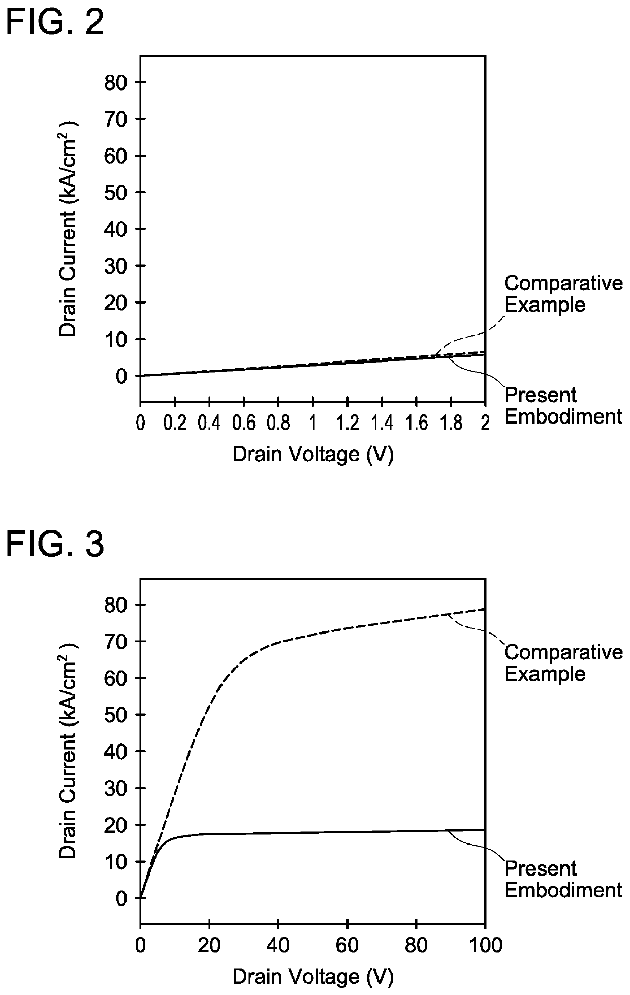
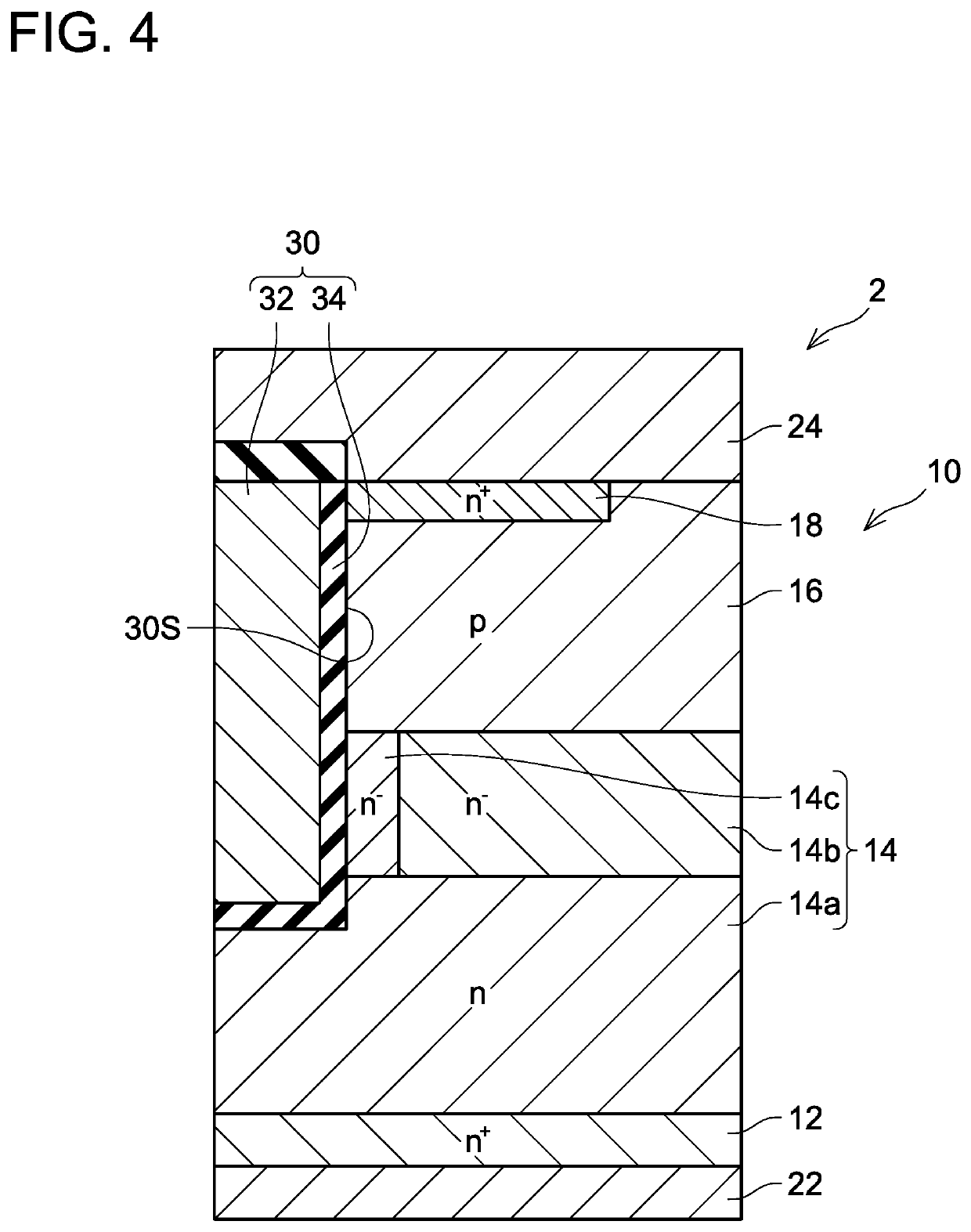
[0005]In an embodiment disclosed herein, a semiconductor device may comprise a semiconductor layer; and a trench gate extending from a front surface of the semiconductor layer toward a back surface thereof. The semiconductor layer may comprise a first semiconductor region of a first conductive type; a second semiconductor region of a second conductive type provided above the first semiconductor region and facing a side surface of the trench gate; and a third semiconductor region of the first conductive type provided above the second semiconductor region, separated from the first semiconductor region by the second semiconductor region, and facing the side surface of the trench gate. The first semiconductor region may comprise: a lower semiconductor region; and an upper semiconductor region disposed between the lower semiconductor region and the second semiconductor region and having a lower impurity concentration than the lower semiconductor region. The upper semiconductor region may be disposed at a shallower position than the trench gate and face the side surface of the trench gate. In the semiconductor device with such a configuration, the presence of the upper semiconductor region between the lower semiconductor region and the second semiconductor region enables suppression of an increase in an on-resistance in a normal operation as well as reduction in saturated current generated when a short circuit occurs.

Problems solved by technology

However, such an increase in the channel resistance increases an on-resistance in a normal operation.

Method used


Image

  • Power semiconductor device
  • Power semiconductor device
  • Power semiconductor device

Examples


Embodiment Construction

[0010]Representative, non-limiting examples of the present disclosure will now be described in further detail with reference to the attached drawings. This detailed description is merely intended to teach a person of skill in the art further details for practicing preferred aspects of the present teachings and is not intended to limit the scope of the present disclosure. Furthermore, each of the additional features and teachings disclosed below may be utilized separately or in conjunction with other features and teachings to provide improved semiconductor devices, as well as methods for using and manufacturing the same.

[0011]Moreover, combinations of features and steps disclosed in the following detailed description may not be necessary to practice the present disclosure in the broadest sense, and are instead taught merely to particularly describe representative examples of the present disclosure. Furthermore, various features of the above-described and below-described representativ...


PUM

PropertyMeasurementUnit
widthaaaaaaaaaa
depth D1aaaaaaaaaa
distanceaaaaaaaaaa

Abstract

A semiconductor device may include: a semiconductor layer; and a trench gate. The semiconductor layer may include: a first semiconductor region of a first conductive type; a second semiconductor region of a second conductive type provided above the first semiconductor region and facing a side surface of the trench gate; and a third semiconductor region of the first conductive type provided above the second semiconductor region, separated from the first semiconductor region by the second semiconductor region, and facing the side surface of the trench gate. The first semiconductor region may include: a lower semiconductor region; and an upper semiconductor region disposed between the lower semiconductor region and the second semiconductor region and having a lower impurity concentration than the lower semiconductor region. The upper semiconductor region may be disposed at a shallower position than the trench gate and face the side surface of the trench gate.

Description

CROSS-REFERENCE TO RELATED APPLICATION[0001]This application claims priority to Japanese Patent Application No. 2018-070960 filed on Apr. 2, 2018, the contents of which are hereby incorporated by reference into the present application.TECHNICAL FIELD[0002]The present disclosure relates to a semiconductor device.DESCRIPTION OF RELATED ART[0003]A semiconductor device is used in a power conversion device such as an inverter, and is used to control power supply to a load such as a motor. As described in International Publication No. WO 2016 / 067374, the load may be short-circuited due to various reasons. In such cases, the semiconductor device is exposed to stress of high voltage and large current. The stress of high voltage and large current when the load is short-circuited may bring forth a risk of thermal destruction of the semiconductor device.BRIEF SUMMARY[0004]Thus, a technique that reduces saturated current generated when a short circuit occurs to improve a short circuit tolerance...

Claims


Application Information

Patent Timeline
Patent Type & Authority Patents(United States)
IPC IPC(8): H01L29/78H01L29/423H01L29/10H01L29/739H01L29/08
CPCH01L29/7397H01L29/0865H01L29/1095H01L29/4236H01L29/7813H01L29/0878
Inventor UESUGI, TSUTOMUKANECHIKA, MASAKAZU
Owner TOYOTA CENT RES & DEV LAB INC
Learn More