
Circuits, architectures, apparatuses, systems, and methods for ESD protection of integrated circuits having multiple power rails

Inactive Publication Date: 2010-11-23
MARVELL INT LTD
View PDF3 Cites 16 Cited by
  • Summary
  • Abstract
  • Description
  • Claims
  • Application Information

AI Technical Summary

Benefits of technology

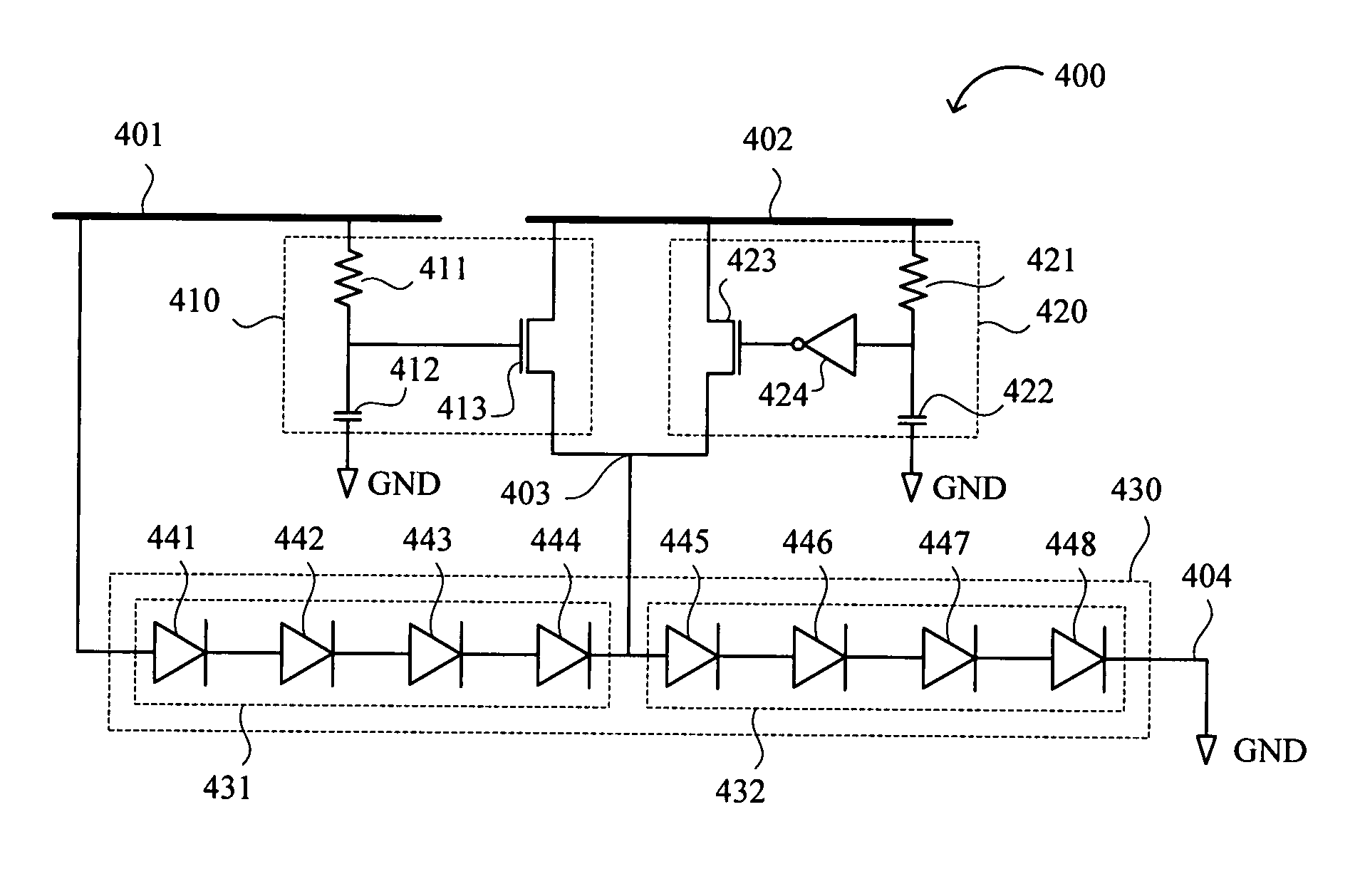
[0024]The present invention advantageously provides ESD protection that can be shared by independent power supply rails with minimal current leakage through the ESD device, thereby reducing the number of ESD devices in and / or on an integrated circuit device. These and other advantages of the present invention will become apparent from the detailed description of embodiments below.

Problems solved by technology

It is generally recognized that integrated circuits are susceptible to damage from electrostatic discharge (ESD).
Such damage generally occurs when current and / or voltage ratings of devices in an integrated circuit are exceeded.
With scaled-down device dimensions, shallow junction depths, thinner gate oxides, lightly doped drain (LDD) structures, and the use of salicide process technology, integrated circuits generally become more susceptible to ESD damage.
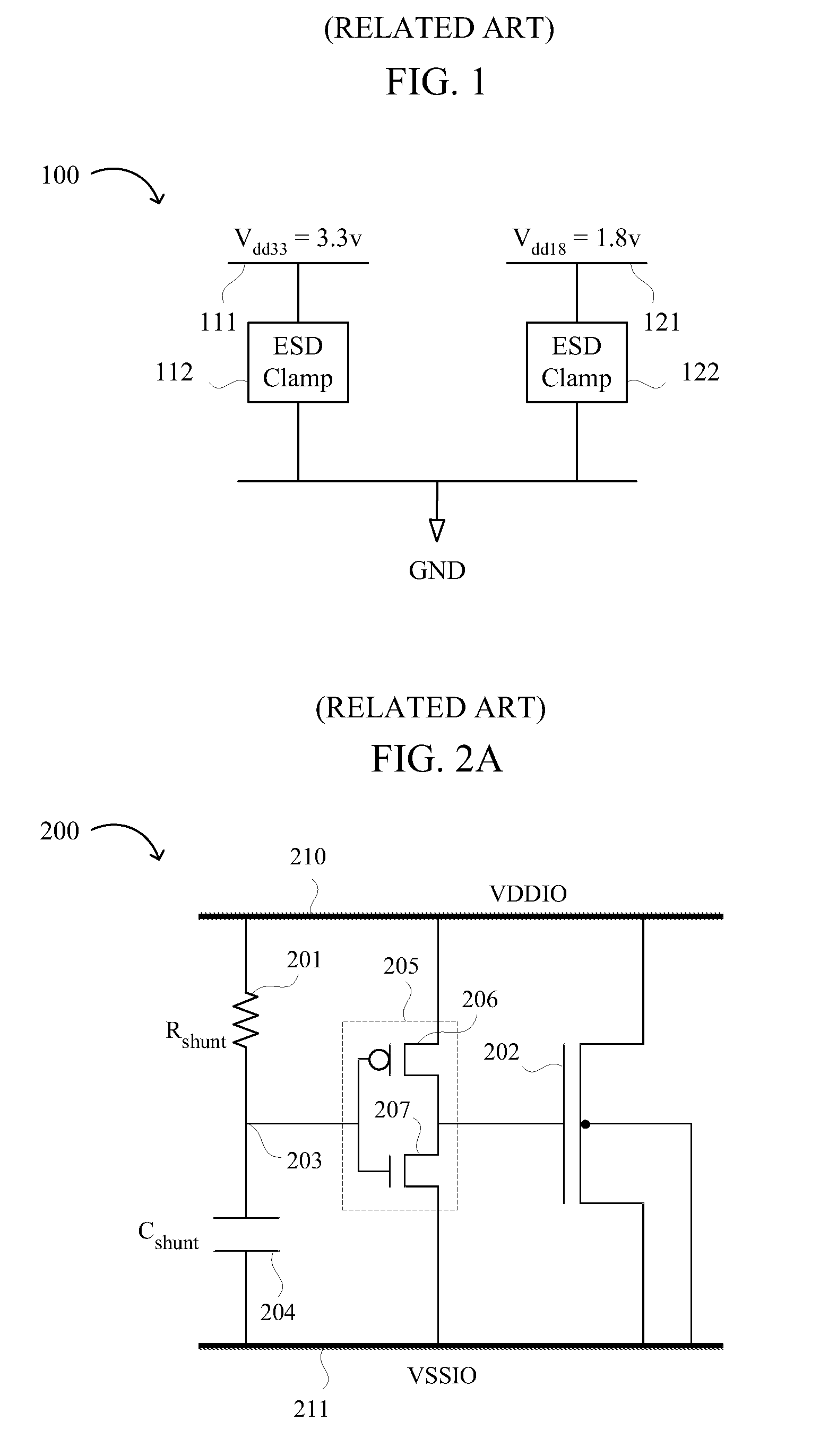
This becomes more severe when the integrated circuit consists of multiple independently-powered circuit sections (e.g., sections of the integrated circuit having isolated power rails).
For example, when a human handler inadvertently touches the leads of an IC and passes such a high static charge to an input buffer on the IC, significant (and sometimes fatal) damage can be done to the IC if the IC is without some kind of protection against such ESD.
A CDM event can be more destructive than an HBM event for some devices.
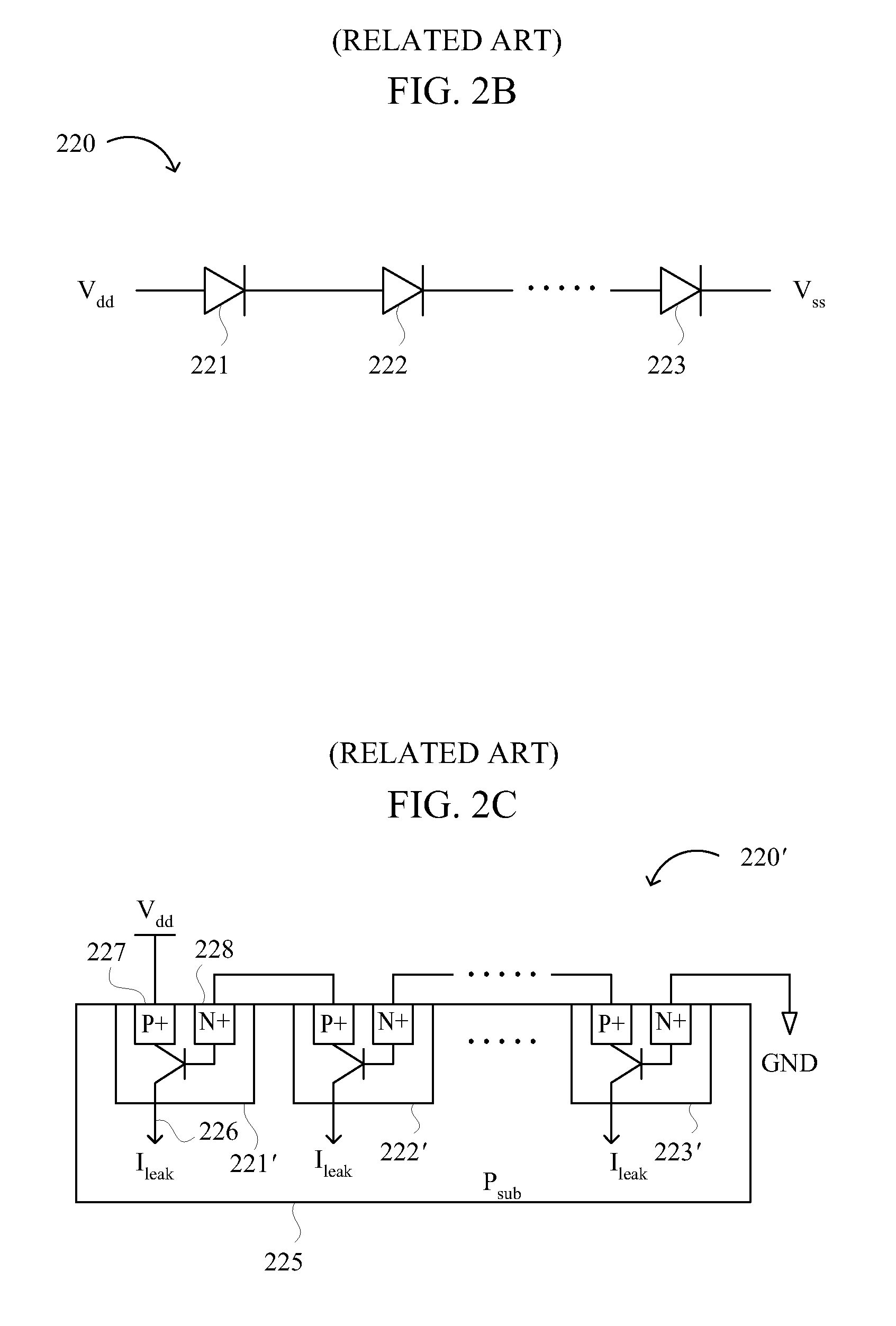
Diode chain 220′ is also subject to current leakage during normal operation.
In addition, ESD protective structures may consume a relatively substantial portion of a semiconductor die that is manufactured using modern manufacturing processes (e.g., 0.13 μm, 90 nm, 65 nm, etc.).
Thus, larger structures such as ESD clamps may be relatively more expensive to produce in a smaller manufacturing process than in an older manufacturing process (e.g., 0.18 μm, 0.25 μm, etc.).

Method used


Image

  • Circuits, architectures, apparatuses, systems, and methods for ESD protection of integrated circuits having multiple power rails
  • Circuits, architectures, apparatuses, systems, and methods for ESD protection of integrated circuits having multiple power rails
  • Circuits, architectures, apparatuses, systems, and methods for ESD protection of integrated circuits having multiple power rails

Examples


Embodiment Construction

[0040]Reference will now be made in detail to embodiments of the invention, examples of which are illustrated in the accompanying drawings. While the invention will be described in conjunction with the embodiments, it will be understood that they are not intended to limit the invention to these embodiments. On the contrary, the embodiments of the invention are intended to cover alternatives, modifications, and equivalents that may be included within the spirit and scope of the appended claims. Furthermore, in the following detailed description of the embodiments of the present invention, numerous specific details are set forth in order to provide a thorough understanding of the present invention. However, it will be readily apparent to one skilled in the art that embodiments of the present invention may be practiced without these specific details. In other instances, well-known methods, procedures, components, and circuits have not been described in detail so as not to unnecessarily...


PUM


Abstract

Circuits, systems, and methods for protecting an integrated circuit device having a first power rail and a second power rail from electrostatic discharge (ESD) events. The ESD protection circuit generally comprises an ESD shunt device coupled to the first power rail and a ground potential, a bias circuit configured to provide a bias voltage to the ESD shunt device during a normal mode of operation and to disable the bias voltage during an ESD event on the first power rail, and an isolation circuit configured to isolate the second power rail from the ESD shunt device during the normal mode of operation and to couple the second power rail to the ESD shunt device during an ESD event on the second power rail. The present invention advantageously provides ESD protection that can be shared by independent power supply rails with minimal current leakage through the ESD device, thereby reducing the total number of ESD protection circuits on a mixed supply integrated circuit device.

Description

RELATED APPLICATIONS[0001]This application claims the benefit of U.S. Provisional Application No. 60 / 828,698, filed Oct. 9, 2006, incorporated herein by reference in its entirety.FIELD OF THE INVENTION[0002]The present invention generally relates to the field of electrostatic discharge (ESD) protection. More specifically, embodiments of the present invention pertain to circuits, architectures, systems, and methods for ESD protection of integrated circuits having multiple power rails.DISCUSSION OF THE BACKGROUND[0003]It is generally recognized that integrated circuits are susceptible to damage from electrostatic discharge (ESD). Such damage generally occurs when current and / or voltage ratings of devices in an integrated circuit are exceeded.[0004]Progress in VLSI technology today has resulted in smaller and smaller integrated circuit geometries in integrated circuits. With scaled-down device dimensions, shallow junction depths, thinner gate oxides, lightly doped drain (LDD) structure...

Claims


Application Information

Patent Timeline
IPC IPC(8): H02H9/00
CPCH01L27/0285
Inventor CHAN, YING POH
Owner MARVELL INT LTD
Learn More