Semiconductor integrated circuit device and inspection method therefor

a technology of integrated circuit and integrated circuit device, which is applied in the direction of error detection/correction, instruments, computing, etc., can solve the problems of limited number of pads connected to external measurement apparatus used for measurement, limited area provided for test circuit, and limited number of measurements, etc., to achieve the effect of reducing yield

Inactive Publication Date: 2010-11-30
PANASONIC CORP
View PDF5 Cites 1 Cited by
  • Summary
  • Abstract
  • Description
  • Claims
  • Application Information

AI Technical Summary

Benefits of technology

[0018]According to the first semiconductor integrated circuit device, the magnitude comparison circuit makes the magnitude comparison of the electrical characteristic between the devices under test, which makes it possible to verify quality of the fabrication process, that is, stability of the fabrication process within a reasonable time.
[0048]As described above, the semiconductor integrated circuit device and the inspection method therefore according to the present invention allow verifying the fabrication process within a short time, which makes it possible to find a decrease in yield at an early stage, the decrease being caused by variation in fabrication process.

Problems solved by technology

Therefore, a region provided for the test circuit is limited in area.
However, as described above, the number of measurements is limited in such a test circuit that is simply and conveniently structured to be formed in the scribe line region.
Since number of pads which are connected to an external measurement apparatus used for measurement is also limited, it is difficult to measure a number of test circuits.
If a whole area of the semiconductor wafer is measured while changing measurement conditions or the like for every device under test 102, there is a problem that an enormously long inspection time is required.
In a current fabrication process of semiconductor device, cost required for inspection constitutes a large proportion of the whole fabrication cost, and it is not cost-effective to spend such a long time for the inspection.

Method used


Image

  • Semiconductor integrated circuit device and inspection method therefor
  • Semiconductor integrated circuit device and inspection method therefor
  • Semiconductor integrated circuit device and inspection method therefor

Examples


embodiment 1

[0066]Embodiment 1 of the present invention will be described with reference to the drawings.

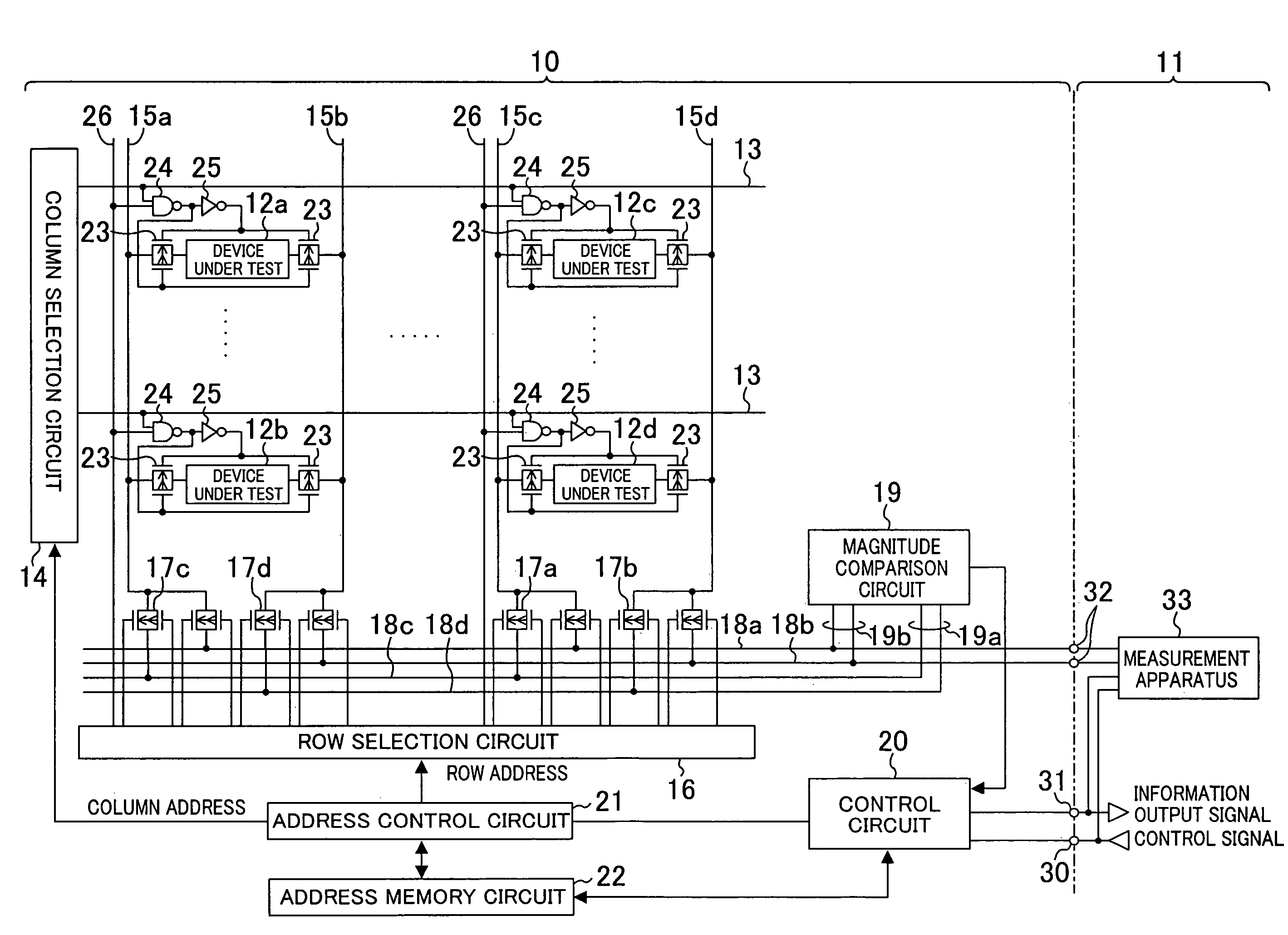
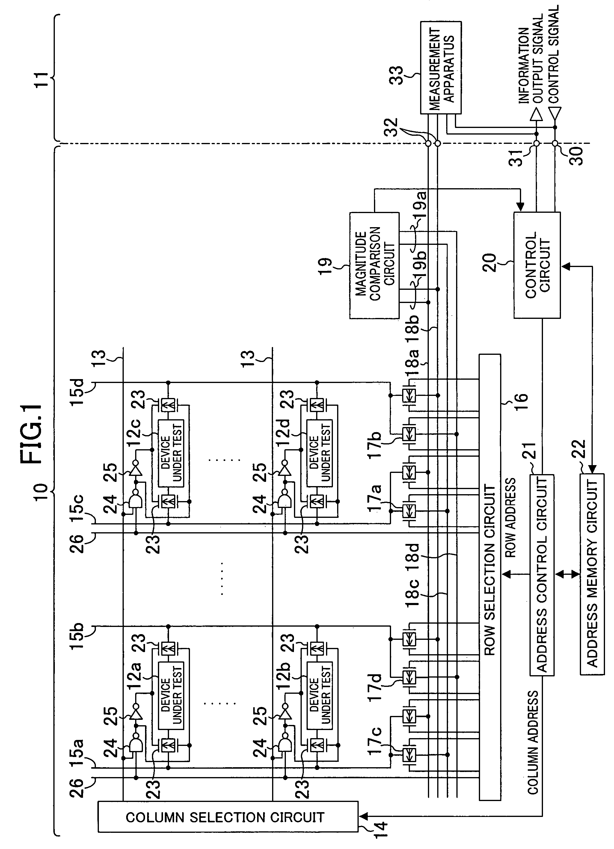
[0067]FIG. 1 is a block diagram illustrating a semiconductor inspection circuit device, which is a semiconductor integrated circuit device of Embodiment 1 of the present invention.

[0068]As shown in FIG. 1, the semiconductor inspection circuit device of Embodiment 1 includes: a plurality of devices under test, such as devices under test 12a, 12b, 12c, and 12d, which are formed, for example, in a scribe line region of a semiconductor wafer 10 and which are arranged in rows and columns; a column selection circuit 14 which is connected to each of the devices under test 12a, 12b, 12c, and 12d via column selection lines 13; a row selection circuit 16 which is connected to each of the devices under test 12a, 12b, 12c, and 12d via row selection lines, such as row selection lines 15a, 15b, 15c, and 15d; a magnitude comparison circuit 19 which is connected to each of the row selection lines 15a, 15b, ...

embodiment 2

[0130]Embodiment 2 of the present invention will be described below with reference to the drawings.

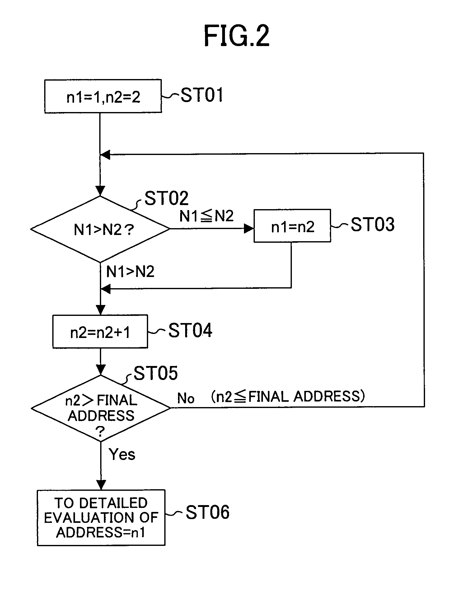
[0131]FIG. 9 shows an exemplary flow chart illustrating a magnitude comparison determination method of a semiconductor inspection circuit device of Embodiment 2 of the present invention.

[0132]In Embodiment 1 of FIG. 1, the method has been explained in which in the self-contained operation mode, an address of a device under test having the maximum value or the minimum value among measured values of an electrical characteristic is extracted, and only the electrical characteristic of the device under test in the address is measured in detail. In Embodiment 2, a memory area of the address memory circuit 22 of Embodiment 1 is further provided and a magnitude comparison determination process illustrated with reference to FIG. 9 is performed, so that it is possible to extract not only an address of a device under test having the maximum value or the minimum value among the measured values, bu...

embodiment 3

[0149]Embodiment 3 of the present invention will be explained below with reference to the drawings.

[0150]FIG. 10 is an exemplary flow chart illustrating a magnitude comparison determination method of a semiconductor inspection circuit device of Embodiment 3 of the present invention.

[0151]Embodiment 2 employs the method as shown in FIG. 9 in which magnitude relations of a plurality of measured values are successively compared, and contents in the addresses n1 through n3 are replaced according to results obtained by the comparison. In order to perform the replacement process of memory contents in the semiconductor inspection circuit device, a temporary memory circuit is required to save information prior to replacement (update). Moreover, a circuit for replacing information is required, which causes an increase in circuit size.

[0152]To cope with the problem, Embodiment 3 is realized such that the magnitude comparison determination can be performed in a simpler circuit structure. As a ...


PUM


Abstract

A semiconductor integrated circuit device includes: a plurality of devices under test formed on a substrate; a selection circuit formed on the substrate which selects two of the plurality of devices under test; a magnitude comparison circuit formed on the substrate which measures an electrical characteristic of the two selected devices under test and makes a magnitude comparison between values of the measured electrical characteristic; an address memory circuit formed on the substrate which stores addresses of the two devices under test between which the magnitude comparison has been made; and a control circuit formed on the substrate and connected to the selection circuit, the magnitude comparison circuit, and the address memory circuit.

Description

CROSS-REFERENCE TO RELATED APPLICATION(S)[0001]This application claims priority under 35 U.S.C. §119(a) on Japanese Patent Application No. 2006-32299 filed on Feb. 9, 2006, the entire contents disclosed in claims, specification, and drawings of which are hereby incorporated by reference.BACKGROUND OF THE INVENTION[0002]1. Field of the Invention[0003]The present invention relates to a semiconductor integrated circuit device and an inspection method therefor. Specifically, the present invention relates to an inspection circuit for controlling fabrication steps of a semiconductor integrated circuit device, to a semiconductor integrated circuit device for evaluating and controlling fabrication processes and for analyzing a failure using the inspection circuit, and to an inspection method therefor.[0004]2. Description of the Prior Art[0005]In order to control the conditions of a fabrication line and to analyze causes of deterioration in characteristic of a semiconductor device in a fabri...

Claims


Application Information

Patent Timeline
Patent Type & Authority Patents(United States)
IPC IPC(8): G06F11/00
CPCG01R31/31722
Inventor MORIWAKI, NOBUYUKIHIRAI, TAKEHIRO
Owner PANASONIC CORP
Why Eureka
Try Eureka