Stack-type semiconductor package, method of forming the same and electronic system including the same

a semiconductor and stacking technology, applied in semiconductor devices, semiconductor/solid-state device details, electrical equipment, etc., can solve the problems of large equipment investment and cost, and achieve the effects of preventing a bridge defect, high pin count, and improving the integration density of stacking

Active Publication Date: 2010-12-14
SAMSUNG ELECTRONICS CO LTD
View PDF15 Cites 71 Cited by
  • Summary
  • Abstract
  • Description
  • Claims
  • Application Information

AI Technical Summary

Benefits of technology

[0007]The present general inventive concept provides a stack-type semiconductor package capable of electrically connecting a lower semiconductor package to an upper semiconductor package, high pin-count for improving integration density in stacking, and preventing a bridge defect that is caused when neighboring solder balls are in contact with each other and a non-wet defect, which causes upper solder balls not to be in contact with lower semiconductor package, a method of forming the same, and an electronic system including the same.

Problems solved by technology

Expanding the capacities and functions of a semiconductor device in a wafer state requires considerable equipment investment and costs in a process of manufacturing wafers, and has a lot of problems that may be caused during the processes to be solved.
However, after semiconductor chips are completely fabricated, integrating two or more semiconductor chips or two or more semiconductor packages into one can be accomplished in a process of assembling a semiconductor package without solving the above problems.

Method used


Image

  • Stack-type semiconductor package, method of forming the same and electronic system including the same
  • Stack-type semiconductor package, method of forming the same and electronic system including the same
  • Stack-type semiconductor package, method of forming the same and electronic system including the same

Examples


Embodiment Construction

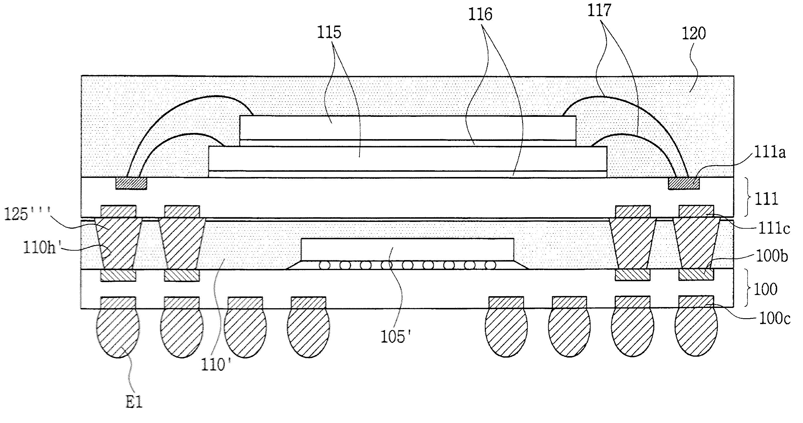
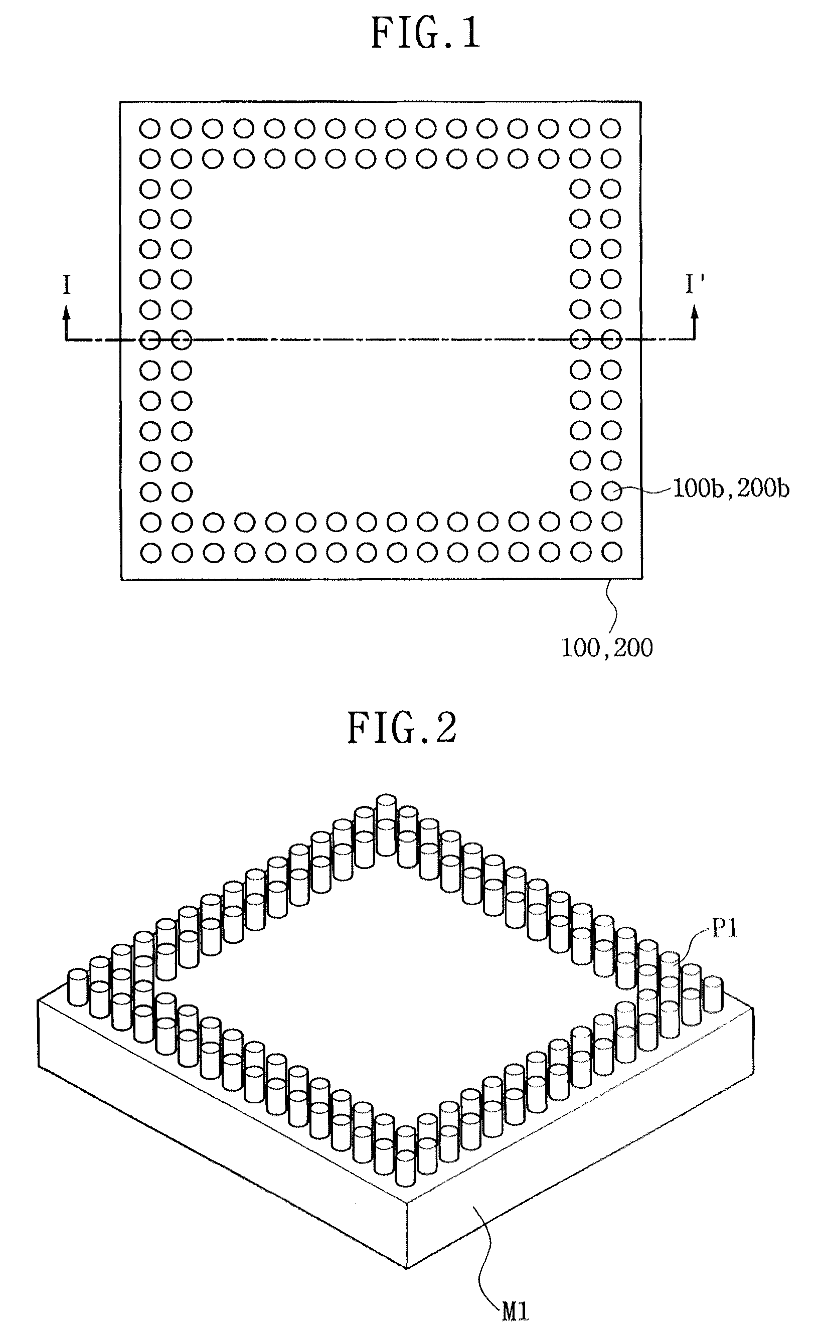
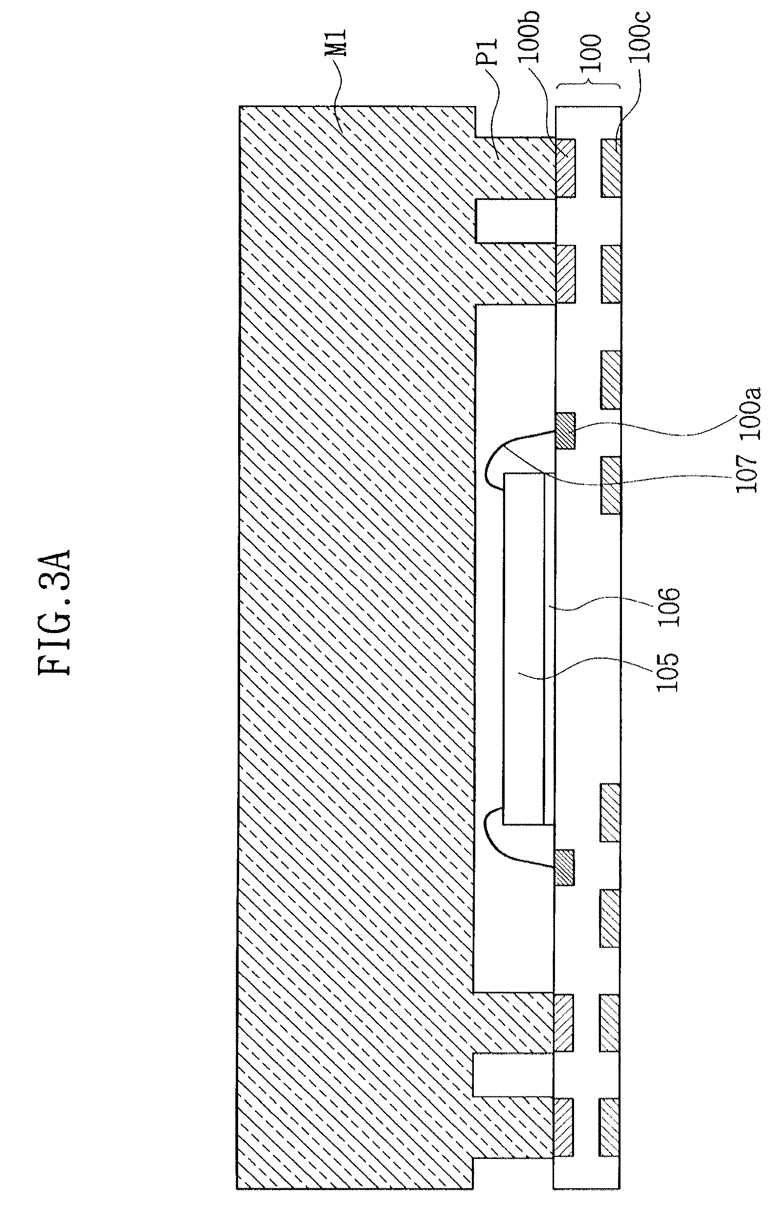
[0052]The present general inventive concept will now be described more fully hereinafter with reference to the accompanying drawings, in which example embodiments of the general inventive concept are illustrated. This general inventive concept may, however, be embodied in different forms and should not be construed as limited to the example embodiments set forth herein. Rather, these example embodiments are provided so that this disclosure will be thorough and complete, and will fully convey the scope of the general inventive concept to those skilled in the art. In the drawings, the thickness of layers and regions may be exaggerated for clarity. Also, when it is referred that a layer is “on” another layer or a substrate, it may be directly formed on another layer or the substrate or a third layer may be interposed therebetween.

[0053]Reference will now be made in detail to embodiments of the present general inventive concept, examples of which are illustrated in the accompanying draw...


PUM


Abstract

A method of forming a stack-type semiconductor package includes preparing a lower printed circuit board including a plurality of interconnections and a plurality of ball lands for connection on an upper surface thereof. One or more first chips, which are electrically connected to the plurality of interconnections and sequentially stacked, are mounted on the lower printed circuit board. A lower molded resin compound is formed on the lower printed circuit board to cover the first chips, and is formed to have via holes exposing the ball lands for connection. An upper chip package, under which solder balls are formed, is aligned so that the solder balls correspond to the via holes of the lower molded resin compound, respectively. The solder balls are reflown to form connection conductors filling the via holes. A stack-type semiconductor package structure and an electronic system including the same are also provided.

Description

CROSS-REFERENCE TO RELATED APPLICATIONS[0001]This application claims priority under 35 U.S.C. §119(a) from Korean Patent Application No. 10-2007-0088363, filed on Aug. 31, 2007, the contents of which are hereby incorporated herein by reference in its entirety.BACKGROUND OF THE INVENTION[0002]1. Field of the Invention[0003]The present general inventive concept relates to a semiconductor package, a method of forming the same, and an electronic system including the same, and more particularly, to a stack-type semiconductor package, a method of forming the same, and an electronic system including the same.[0004]2. Description of the Related Art[0005]In order to expand capacities and functions, integrity density of a semiconductor package is getting increased in a wafer state, and a semiconductor package, in which two or more semiconductor chips or semiconductor packages are integrated into one, is generalized. Expanding the capacities and functions of a semiconductor device in a wafer s...

Claims


Application Information

Patent Timeline
Patent Type & Authority Patents(United States)
IPC IPC(8): H01L21/48H01L21/50
CPCH01L25/0657H01L25/105H01L23/3128H01L24/16H01L24/29H01L24/32H01L24/48H01L2224/16225H01L2224/16227H01L2224/32145H01L2224/32225H01L2224/48091H01L2224/48227H01L2224/73204H01L2224/73265H01L2225/0651H01L2225/06517H01L2225/0652H01L2225/06541H01L2225/06582H01L2924/078H01L2924/15311H01L2924/15331H01L2924/1815H01L2924/19041H01L2924/19042H01L2924/19043H01L2924/00014H01L2224/32245H01L2924/00H01L2924/00012H01L2225/1023H01L2225/1058H01L2924/3512H01L24/73H01L2924/181H01L2224/45099H01L2224/45015H01L2924/207H01L23/12H01L23/28
Inventor KIM, TAE-HUN
Owner SAMSUNG ELECTRONICS CO LTD
Why Eureka
Try Eureka