Thin film transistor, display device and liquid crystal display device and method for manufacturing the same

a thin film transistor and display device technology, applied in semiconductor devices, optics, instruments, etc., can solve the problems of increased processing time, difficult to manufacture a display panel with good productivity, and difficult to handle large substrates

Inactive Publication Date: 2011-01-11
SEMICON ENERGY LAB CO LTD
View PDF22 Cites 67 Cited by
  • Summary
  • Abstract
  • Description
  • Claims
  • Application Information

AI Technical Summary

Benefits of technology

[0036]Patterns other than the conductive film formed in the hole of the insulating film may not necessarily be formed by a method by which a pattern can be selectively formed. Meanwhile, all the patterns may be formed by a method by which a pattern can be selectively formed. The good effect of the invention can be utilized when a pattern is formed in a hole of the insulating film in one step of fabricating a thin film transistor.
[0037]It is a feature of a display device according to the invention that resin is formed around at least one conductor formed on one of two substrates sandwiching liquid crystal.
[0038]Here, a conductor denotes every kind of conductor such as an active element typified by a semiconductor element such as a TFT used for a pixel area or a peripheral circuit area of an active matrix liquid crystal display device; or a gate electrode, gate wiring, a capacitor wiring, a source electrode, a drain electrode, a source wiring, a drain wiring, or a pixel electrode, which is included in a circuit.
[0039]Various materials can be selected corresponding to the use, function, area, or the like of the conductor. Typically, silver (Ag), copper (Cu), gold (Au), nickel (Ni), platinum (Pt), chrome (Cr), tin (Sn), palladium (Pd), iridium (Ir), rhodium (Rh), ruthenium (Ru), rhenium (Re), tungsten (W), aluminum (Al), tantalum (Ta), indium (In), tellurium (Te), molybdenum (Mo), cadmium (Cd), zinc (Zn), iron (Fe), titanium (Ti), silicon (Si), germanium (Ge), zirconium (Zr), barium (Ba), antimonial lead, tin oxide antimony, fluorine dope zinc oxide, carbon (C), graphite, glassy carbon, lithium (Li), beryllium (Be), sodium (Na), magnesium (Mg), potassium (K), calcium (Ca), scandium (Sc), manganese (Mn), zirconium (Zr), gallium (Ga), niobium (Nb), sodium-potassium alloy, a magnesium / copper mixture, a magnesium / silver mixture, a magnesium / aluminum mixture, a magnesium / indium mixture, an aluminum / aluminum oxide mixture, a lithium / aluminum mixture, particles of silver halide or dispersible nanoparticles can be used. Further, indium tin oxide (ITO), zinc oxide (ZnO), zinc oxide added with gallium (GZO), or indium zinc oxide (IZO) in which 2% to 20% of zinc oxide is mixed into indium oxide, organic indium can be used for transparent conductive film. Still further, organotin or titanium nitride can be used for the conductor.
[0040]Silicon (Si) or silicon oxide (SiOx) may be contained in the foregoing conductive material, especially when used to form the transparent conductive film. For example, a conductive material composed of ITO containing silicon oxide (ITSO) can be used. Further, a desired conductive film may be formed by stacking layers formed from these conductive materials.
[0041]Such a conductor includes a semiconductor material such as polysilicon as well as the above metal materials. In the case of a passive liquid crystal display device, an electrode arranged in grid (stripes), a wiring, and the like are given as a conductor.

Problems solved by technology

It is difficult to manufacture a display panel with good productivity with low cost only by a conventional patterning method.
In other words, when a plurality of times of light-exposure is carried out by consecutive light exposure, a processing time is increased and it is difficult to handle large substrates.
Moreover, in a method in which various kinds of films are formed over an entire surface of a substrate and the films are thereafter etched away leaving a small region thereof, there is a problem that higher material costs are spent and a large amount of liquid waste containing heavy metal or the like is required to be processed.
Further, according to the above reference 2, as a wiring becomes thick, discontinuity of a thin film covering the wiring has become a problem.
As a wiring is miniaturized, signal delay due to wiring resistance has become a problem.

Method used


Image

  • Thin film transistor, display device and liquid crystal display device and method for manufacturing the same
  • Thin film transistor, display device and liquid crystal display device and method for manufacturing the same
  • Thin film transistor, display device and liquid crystal display device and method for manufacturing the same

Examples


embodiment mode 1

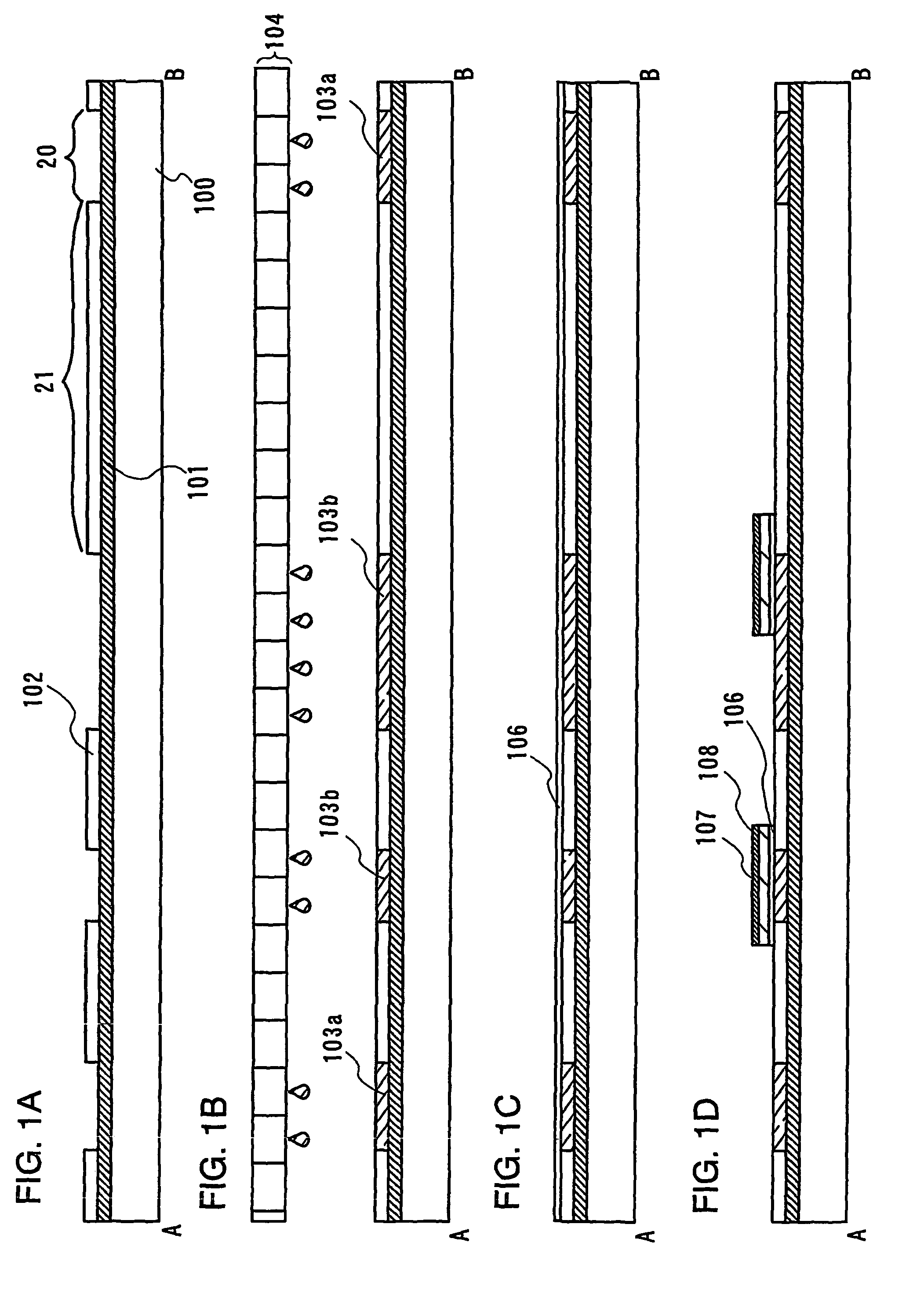
[0120]In this embodiment mode, an example of a method for forming a thin film transistor.

[0121]First, as shown in FIG. 1A, a substrate 100 having an insulating surface is prepared. For example, a glass substrate such as barium borosilicate glass or alumino borosilicate glass; a quartz substrate; a stainless steel substrate, a bulk semiconductor film; or the like can be used for the substrate 100. Further, a substrate formed of a flexible synthetic resin such as acrylic or plastics typified by polyethylene-terephthalate (PET), a polyethylene naphthalate (PEN), and polyethersulfone (PES) generically has low heat-resistant temperature as compared with a substrate formed of another material. However, such a substrate can be used if it can endure a processing temperature of the fabrication process. In particular, in the case of forming a thin film transistor including an amorphous semiconductor film which does not require a heating process for crystallizing a semiconductor film, a substr...

embodiment mode 2

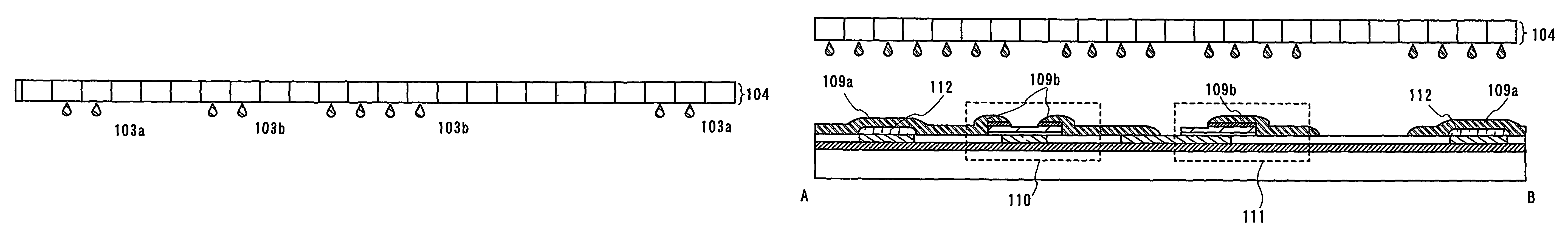
[0177]In this embodiment, the case where the above thin film transistor is used for a pixel area of a display device, a light emitting device, for example will be described.

[0178]The thin film transistor 110 functions as a switch, and the thin film transistor functions as a driver for controlling the luminance intensity of an electroluminescent layer. The source electrode or the drain electrode of the thin film transistor functioning as a switch (a switching TFT) is connected with the gate electrode of the thin film transistor functioning as a driver (a driving TFT).

[0179]The thin film transistors according to this embodiment mode are channel etch type. A substrate mounted with a plurality of such thin film transistors is referred to as a TFT substrate.

[0180]As shown in FIG. 2B, an insulating film serving as an interlayer insulating film 113, an auxiliary wiring, and a conductive film 114 serving as a connection wiring are formed. The conductive film serving as an auxiliary wiring i...

embodiment mode 3

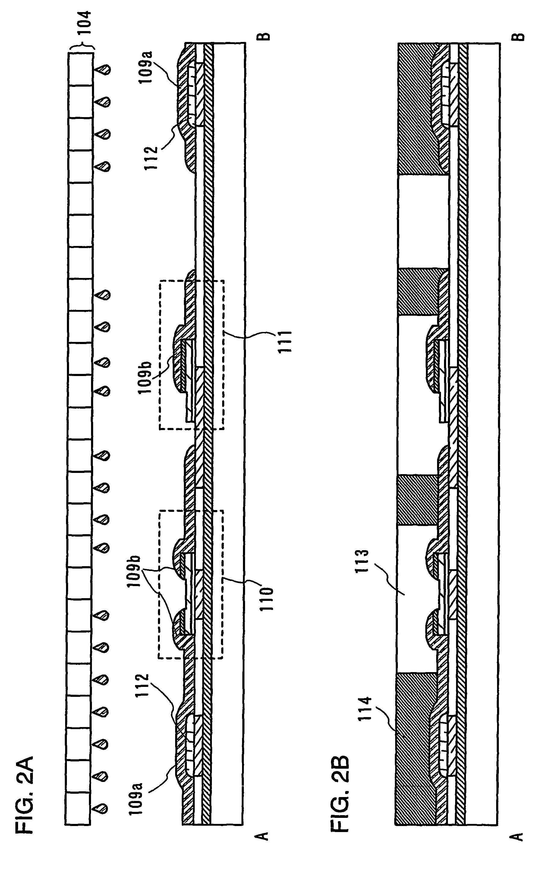
[0221]In this embodiment mode, an example of forming a thin film transistor by a method different from the above embodiment mode will be described. Specifically, an insulating film is formed on a semiconductor region to be a channel region here. The other structure of a thin film transistor is similar to the above embodiment mode; accordingly, the description will be omitted.

[0222]As shown in FIG. 10, as in the above embodiment mode, a base film 101 is formed; insulating films 102, a scan line 103a, and a gate electrode are formed over a substrate 100; and a gate insulating film is formed so as to cover the insulating film, the scan line, and the gate electrode. Thereafter, a semiconductor film is formed on the gate insulating film. On this occasion, the surfaces of the insulating films 102, the scan line 103a, and the gate electrode 103b are trued up and planarized; thus, the gate insulating film can be formed without discontinuity.

[0223]Subsequently, an insulating film 140 serving...


PUM

PropertyMeasurementUnit
depthaaaaaaaaaa
depthaaaaaaaaaa
depthaaaaaaaaaa

Abstract

As a wiring becomes thicker, discontinuity of an insulating film covering the wiring has become a problem. It is difficult to form a wiring with width thin enough for a thin film transistor used for a current high definition display device. As a wiring is made thinner, signal delay due to wiring resistance has become a problem. In view of the above problems, the invention provides a structure in which a conductive film is formed in a hole of an insulating film, and the surfaces of the conductive film and the insulating film are flat. As a result, discontinuity of thin films covering a conductive film and an insulating film can be prevented. A wiring can be made thinner by controlling the width of the hole. Further, a wiring can be made thicker by controlling the depth of the hole.

Description

TECHNICAL FIELD[0001]The present invention relates to methods for fabricating a wiring, a thin film transistor, and a display device, each of which employs a method by which a pattern can be selectively formed. In particular, the invention relates to a display device having an active element such as a transistor formed over a large glass substrate by using a droplet discharge method typified by ink-jet as a method by which a pattern can be selectively formed, and to a fabrication method of the display device. Further, the invention relates to a wiring, a thin film transistor, and a display device which are formed by a method by which a pattern can be selectively formed.BACKGROUND ART[0002]Conventionally, a display panel of a so-called active matrix driving method constituted by a thin film transistor (hereinafter also referred to as a “TFT”) over a glass substrate has been fabricated by patterning various kinds of thin films by a light exposure process using a photomask as well as a...

Claims


Application Information

Patent Timeline
Patent Type & Authority Patents(United States)
IPC IPC(8): G02F1/1368H01L21/336H01L21/288H01L21/28H01L21/768H01L21/77H01L21/84H01L27/12H01L29/786
CPCH01L21/28008H01L21/288H01L21/76838H01L27/1292H01L29/66765H01L29/78669H01L29/78678H01L2224/73265H01L29/42384
Inventor YAMAZAKI, SHUNPEIMAEKAWA, SHINJIKANNO, YOHEI
Owner SEMICON ENERGY LAB CO LTD
Why Eureka
Try Eureka